Introduction to SMT Stencils
Surface Mount Technology (SMT) has revolutionized the electronics manufacturing industry by enabling the production of smaller, faster, and more efficient electronic devices. One of the critical components in the SMT Assembly process is the solder paste stencil, also known as the SMT stencil. This article will provide an in-depth look at SMT stencils, their types, materials, design considerations, and best practices for optimal results.
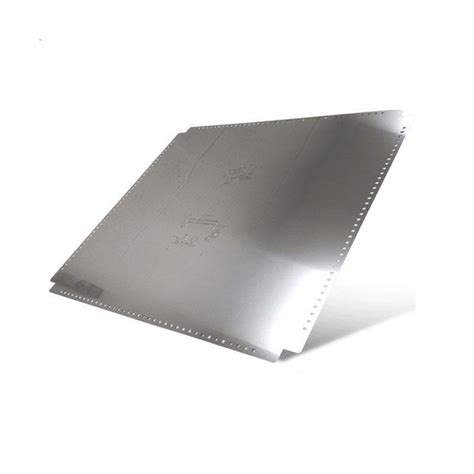
What is an SMT Stencil?
An SMT stencil is a thin metal sheet with precisely cut openings that correspond to the pads on a printed circuit board (PCB). The stencil is used to apply solder paste onto the PCB pads before placing the surface mount components. The solder paste deposited through the stencil openings ensures a precise and uniform amount of solder is applied to each pad, resulting in reliable solder joints after the reflow process.
Types of SMT Stencils
There are several types of SMT stencils available, each with its own advantages and disadvantages. The choice of stencil type depends on factors such as the PCB design, component sizes, and production requirements.
Laser-Cut Stencils
Laser-cut stencils are created using a high-powered laser to cut the openings in the stencil material. This method offers high precision and is suitable for fine-pitch components and intricate designs. Laser-cut stencils are typically made from stainless steel and have a long lifespan.
Chemical-Etched Stencils
Chemical-etched stencils are manufactured by selectively removing material from a metal sheet using a chemical etching process. This method is cost-effective for simple designs and larger apertures. However, chemical-etched stencils may not achieve the same level of precision as laser-cut stencils.
Electroformed Stencils
Electroformed stencils are created by electroplating nickel onto a photoresist-patterned substrate. This process allows for the creation of highly precise and uniform apertures, making it suitable for ultra-fine pitch applications. Electroformed stencils are generally more expensive than laser-cut or chemical-etched stencils.

SMT Stencil Materials
The choice of material for an SMT stencil is crucial to ensure optimal performance and durability. The most common materials used for SMT stencils are:
Stainless Steel
Stainless steel is the most widely used material for SMT stencils due to its durability, stability, and resistance to wear. It is suitable for a wide range of applications and offers excellent paste release properties.
Nickel
Nickel stencils are known for their exceptional durability and resistance to corrosion. They are often used in high-volume production environments and for applications requiring frequent cleaning.
Polyimide
Polyimide stencils, also known as polymer stencils, are made from a flexible, non-metallic material. They are suitable for applications with irregular surfaces or where a conformable stencil is required. Polyimide stencils are less durable than metal stencils and are typically used for prototyping or low-volume production.

SMT Stencil Design Considerations
Designing an effective SMT stencil involves several key considerations to ensure optimal solder paste deposition and prevent common issues such as bridging, insufficient solder, or poor paste release.
Aperture Size and Shape
The size and shape of the stencil apertures directly affect the amount of solder paste deposited onto the PCB pads. Aperture dimensions should be carefully calculated based on the pad size, component pitch, and solder paste properties. Common aperture shapes include square, rectangular, and circular.
Stencil Thickness
The thickness of the SMT stencil determines the volume of solder paste deposited. Thicker stencils deposit more paste, while thinner stencils deposit less. The optimal stencil thickness depends on factors such as the component size, pitch, and solder paste type. Common stencil thicknesses range from 0.1 mm to 0.2 mm (4 to 8 mils).
Aperture Wall Angle
The aperture wall angle, also known as the sidewall angle, affects the release of solder paste from the stencil. A trapezoidal aperture shape with a wall angle of 5° to 7° is recommended for optimal paste release and to prevent clogging.
Fiducial Marks and Alignment Features
Fiducial marks and alignment features are essential for accurately aligning the stencil with the PCB. These features ensure precise registration between the stencil apertures and the PCB pads, minimizing alignment errors and improving the overall print quality.

Stencil Printing Process
The stencil printing process is a critical step in SMT assembly, as it directly affects the quality and reliability of the solder joints. The process involves the following steps:
-
Stencil Alignment: The stencil is aligned with the PCB using fiducial marks and alignment features.
-
Solder Paste Application: Solder paste is dispensed onto the stencil and spread across the surface using a squeegee blade.
-
Paste Deposition: As the squeegee blade moves across the stencil, solder paste is forced through the apertures and onto the PCB pads.
-
Stencil Separation: The stencil is carefully lifted from the PCB, leaving precise deposits of solder paste on the pads.
-
Inspection: The printed PCB is inspected for defects such as bridging, insufficient solder, or misaligned deposits.
Squeegee Blades
Squeegee blades are used to spread the solder paste across the stencil and force it through the apertures. The choice of squeegee blade material, hardness, and profile affects the print quality and consistency.
| Squeegee Material | Advantages | Disadvantages |
|---|---|---|
| Metal | Durable, suitable for high-volume production | Can damage stencil, may cause scooping |
| Polyurethane | Softer, less likely to damage stencil | Less durable, may require frequent replacement |
| Composite | Combines benefits of metal and polyurethane | Higher cost compared to other materials |
Solder Paste Properties
The properties of the solder paste used in the stencil printing process significantly influence the print quality and solder joint reliability. Key solder paste properties include:
- Viscosity: Affects the flow and release of the paste through the stencil apertures.
- Particle Size: Determines the minimum aperture size and influences the print resolution.
- Flux Activity: Impacts the wetting and spreading of the solder paste on the PCB pads.
Stencil Cleaning and Maintenance
Regular cleaning and maintenance of SMT stencils are essential to ensure consistent print quality and extend the stencil’s lifespan. Solder paste residue, debris, and oxidation can accumulate on the stencil surface and in the apertures, leading to printing defects.
Understencil Cleaning
Understencil cleaning is performed during the printing process to remove excess solder paste and prevent the buildup of residue. This is typically done using a solvent-impregnated wiper or an automated understencil cleaning system.
Periodic Deep Cleaning
Periodic deep cleaning is necessary to remove stubborn residue and oxidation from the stencil surface and apertures. This process involves the use of specialized cleaning agents and ultrasonic cleaning equipment. The frequency of deep cleaning depends on factors such as the solder paste type, printing volume, and environmental conditions.
Stencil Storage
Proper storage of SMT stencils is crucial to prevent damage and contamination. Stencils should be stored in a clean, dry environment, away from direct sunlight and extreme temperatures. Stencil storage racks or cabinets are recommended to keep stencils organized and protected.
Best Practices for Optimal SMT Stencil Performance
To achieve the best results with SMT stencils, consider the following best practices:
-
Collaborate closely with your PCB designer and stencil manufacturer to ensure optimal stencil design and specifications.
-
Use high-quality solder paste with properties suitable for your specific application and stencil design.
-
Implement a robust stencil cleaning and maintenance program to ensure consistent print quality and extend stencil life.
-
Regularly inspect and monitor the printed PCBs for defects and make necessary adjustments to the stencil design or printing process.
-
Invest in training and education for your SMT assembly team to ensure they are knowledgeable about stencil printing best practices and troubleshooting techniques.
Frequently Asked Questions (FAQ)
1. What is the difference between a solder paste stencil and a solder mask?
A solder paste stencil is used to apply solder paste onto the PCB pads during the SMT assembly process. In contrast, a solder mask is a protective layer applied to the PCB surface to prevent solder bridging and provide insulation between conductive traces.
2. Can SMT stencils be reused?
Yes, SMT stencils can be reused multiple times with proper cleaning and maintenance. However, the lifespan of a stencil depends on factors such as the material, printing volume, and handling practices.
3. How do I choose the right stencil thickness for my application?
The choice of stencil thickness depends on several factors, including the component size, pitch, and solder paste type. As a general guideline, use thinner stencils (0.1 mm to 0.15 mm) for fine-pitch components and thicker stencils (0.15 mm to 0.2 mm) for larger components.
4. What causes solder paste bridging, and how can it be prevented?
Solder paste bridging occurs when excess solder paste connects adjacent pads, creating a short circuit. Bridging can be caused by factors such as improper stencil design, incorrect solder paste properties, or poor printing parameters. To prevent bridging, ensure proper stencil aperture design, use solder paste with suitable properties, and optimize printing parameters such as squeegee pressure and speed.
5. How often should I clean my SMT stencil?
The frequency of stencil cleaning depends on the solder paste type, printing volume, and environmental conditions. As a general rule, perform understencil cleaning every 1-4 hours of continuous printing and conduct periodic deep cleaning as needed based on visual inspection of the stencil surface and print quality.
Conclusion
SMT stencils play a critical role in the surface mount technology assembly process, ensuring precise and consistent solder paste deposition for reliable solder joints. By understanding the types, materials, design considerations, and best practices associated with SMT stencils, electronics manufacturers can optimize their SMT assembly process and produce high-quality, reliable electronic devices.
As the electronics industry continues to evolve, with smaller components and more complex designs, the importance of SMT stencils will only continue to grow. Staying up-to-date with the latest advancements in stencil technology and best practices is essential for maintaining a competitive edge in the fast-paced world of electronics manufacturing.


Leave a Reply