Introduction to PLCC Packages
PLCC (Plastic Leaded Chip Carrier) packages are a type of surface-mount integrated circuit package that has been widely used in electronics manufacturing for several decades. These packages offer a compact and reliable solution for housing various types of integrated circuits, such as microprocessors, memory chips, and application-specific integrated circuits (ASICs).
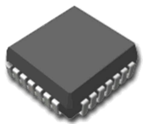
What are PLCC Packages?
PLCC packages are characterized by their rectangular or square shape and the presence of J-shaped leads on all four sides of the package. These leads are bent downwards and outwards, allowing the package to be easily soldered onto a printed circuit board (PCB) using surface-mount technology (SMT).
The main components of a PLCC package include:
- The integrated circuit (IC) chip
- The lead frame, which provides electrical connections between the chip and the PCB
- The plastic encapsulant, which protects the chip and the lead frame from environmental factors
Advantages of PLCC Packages
PLCC packages offer several advantages over other types of IC packages, such as:
- Compact size: PLCC packages have a smaller footprint compared to through-hole packages, allowing for higher component density on PCBs.
- Improved thermal performance: The J-shaped leads of PLCC packages provide a larger surface area for heat dissipation, which helps in managing the thermal performance of the IC.
- Enhanced reliability: The plastic encapsulant protects the IC chip from moisture, dust, and other environmental factors, improving the overall reliability of the device.
- Easier handling and assembly: The J-shaped leads of PLCC packages make them easier to handle and assemble using SMT processes, reducing manufacturing costs and time.
PLCC Package Variants
There are several variants of PLCC packages, each designed to cater to specific requirements and applications. Some of the most common PLCC package variants include:
PLCC-20, PLCC-28, PLCC-44, and PLCC-68
These variants differ in the number of leads they have, with the number in the name indicating the total number of leads. For example, a PLCC-20 package has 20 leads, while a PLCC-68 package has 68 leads. The choice of the package variant depends on the complexity and pin count of the IC being housed.
PLCC-J and PLCC-A
PLCC-J and PLCC-A are two different lead styles for PLCC packages. PLCC-J packages have J-shaped leads, which is the most common lead style. PLCC-A packages, on the other hand, have angled leads that are bent downwards at a 45-degree angle. PLCC-A packages are less common and are typically used in applications that require a lower profile or a specific lead configuration.
EIAJ PLCC Packages
EIAJ (Electronic Industries Association of Japan) PLCC packages are a variant that follows the standards set by the EIAJ. These packages have similar characteristics to standard PLCC packages but may have slightly different dimensions or lead configurations to comply with EIAJ guidelines.

PLCC Package Dimensions and Pinouts
The dimensions and pinouts of PLCC packages vary depending on the specific variant and the number of leads. It is essential to refer to the manufacturer’s datasheet or package specification to obtain accurate information about the dimensions and pinouts of a particular PLCC package.
However, some general guidelines can be followed when working with PLCC packages:
- The pitch, or the distance between the centers of adjacent leads, is typically 1.27 mm (0.05 inches) for most PLCC packages.
- The overall dimensions of the package, including the length, width, and height, depend on the number of leads and the specific variant.
- The pinout, or the assignment of specific functions to each lead, varies depending on the IC being housed in the package. It is crucial to refer to the IC’s datasheet to determine the correct pinout for a given application.
Here’s an example table showing the typical dimensions for some common PLCC package variants:
| Package Variant | Length (mm) | Width (mm) | Height (mm) | Pitch (mm) |
|---|---|---|---|---|
| PLCC-20 | 8.89 | 8.89 | 4.57 | 1.27 |
| PLCC-28 | 11.43 | 11.43 | 4.57 | 1.27 |
| PLCC-44 | 16.51 | 16.51 | 4.57 | 1.27 |
| PLCC-68 | 24.13 | 24.13 | 4.57 | 1.27 |

PCB Design Considerations for PLCC Packages
When designing a PCB for PLCC packages, several factors need to be considered to ensure proper functionality and reliability:
Footprint Design
The footprint is the pattern of pads and holes on the PCB that corresponds to the leads of the PLCC package. The footprint must be designed accurately to ensure proper soldering and alignment of the package. Key aspects of footprint design include:
- Pad size and shape: The pads should be large enough to accommodate the J-shaped leads of the PLCC package and provide sufficient area for soldering. Typically, oval-shaped pads are used to allow for some misalignment during assembly.
- Pad spacing: The spacing between the pads should match the pitch of the PLCC package leads, which is typically 1.27 mm.
- Solder mask opening: The solder mask opening around the pads should be large enough to expose the entire pad area and allow for proper soldering.
Thermal Management
PLCC packages dissipate heat during operation, and it is essential to provide adequate thermal management to prevent overheating and ensure reliable performance. Some techniques for thermal management include:
- Copper pours: Adding large areas of copper on the PCB around the PLCC package helps in spreading the heat and improving thermal dissipation.
- Thermal vias: Placing thermal vias underneath the PLCC package helps in conducting heat from the package to the other layers of the PCB and eventually to the heatsink or ambient environment.
- Heatsinks: In applications with high power dissipation, external heatsinks can be attached to the PLCC package to improve thermal performance.
Signal Integrity
Proper signal integrity is crucial for the reliable operation of ICs in PLCC packages. Some guidelines for maintaining signal integrity include:
- Minimizing trace lengths: Keeping the traces between the PLCC package and other components as short as possible helps in reducing signal reflections and improving signal quality.
- Impedance matching: Ensuring proper impedance matching between the traces and the IC’s input/output pins helps in minimizing signal reflections and improving signal integrity.
- Proper grounding: Providing a solid ground plane and proper grounding techniques helps in reducing noise and improving signal quality.

PLCC Socket and Adapter Options
In some applications, it may be necessary to use PLCC sockets or adapters to interface with PLCC packages. PLCC sockets and adapters provide a means to connect PLCC packages to a PCB without soldering them directly.
PLCC Sockets
PLCC sockets are designed to hold PLCC packages and provide electrical connections between the package leads and the PCB. These sockets are useful in applications where the PLCC package needs to be replaceable or where soldering is not feasible. PLCC sockets come in various sizes to accommodate different PLCC package variants and can be surface-mounted or through-hole mounted on the PCB.
PLCC Adapters
PLCC adapters are used to convert PLCC packages to other package types or to provide compatibility with different PCB layouts. Some common types of PLCC adapters include:
- PLCC to DIP adapters: These adapters allow PLCC packages to be used with breadboards or through-hole PCBs that are designed for DIP (Dual Inline Package) ICs.
- PLCC to PGA adapters: These adapters convert PLCC packages to PGA (Pin Grid Array) packages, which can be useful in certain applications or for compatibility with specific PCB layouts.
- PLCC to QFP adapters: These adapters convert PLCC packages to QFP (Quad Flat Package) packages, which can be useful for adapting older PLCC-based designs to newer QFP-based components.
Handling and Assembly of PLCC Packages
Proper handling and assembly techniques are essential to ensure the reliability and longevity of PLCC packages in electronic assemblies.
Handling Precautions
PLCC packages, like most electronic components, are sensitive to electrostatic discharge (ESD) and require proper handling to prevent damage. Some precautions to take when handling PLCC packages include:
- Use ESD-safe workstations and tools: Always handle PLCC packages in an ESD-protected environment, using ESD-safe mats, wrist straps, and grounded tools.
- Avoid touching the leads: Minimize contact with the leads of the PLCC package to prevent contamination, bending, or damage.
- Store in ESD-safe packaging: When not in use, store PLCC packages in ESD-safe bags or containers to protect them from ESD and physical damage.
Assembly Techniques
The assembly of PLCC packages onto PCBs typically involves surface-mount technology (SMT) processes. Some key aspects of PLCC package assembly include:
- Solder paste application: Apply solder paste to the pads on the PCB using a stencil or syringe. The solder paste should be of the appropriate type and amount for the specific PLCC package and PCB design.
- Component placement: Place the PLCC package onto the PCB, ensuring proper alignment with the pads. Automated pick-and-place machines are often used for high-volume production, while manual placement can be used for prototyping or low-volume assembly.
- Reflow soldering: After placement, the PCB is subjected to a reflow soldering process, where the solder paste is heated to its melting point, forming a strong electrical and mechanical bond between the PLCC package leads and the PCB pads. Reflow soldering can be done using convection ovens, infrared ovens, or vapor phase systems.
- Inspection and testing: After soldering, the assembled PCB should be inspected for proper alignment, solder joint quality, and any defects. Electrical testing can also be performed to verify the functionality of the PLCC package and the overall assembly.
Common Applications of PLCC Packages
PLCC packages are used in a wide range of electronic applications, spanning various industries and sectors. Some common applications include:
- Consumer electronics: PLCC packages are used in devices such as smartphones, tablets, laptops, televisions, and gaming consoles.
- Automotive electronics: In the automotive industry, PLCC packages are used in engine control units, infotainment systems, and other electronic modules.
- Industrial automation: PLCC packages are used in programmable logic controllers (PLCs), sensors, and other industrial automation components.
- Medical devices: In medical electronics, PLCC packages are used in monitoring equipment, diagnostic devices, and implantable devices.
- Telecommunications: PLCC packages are used in routers, switches, and other networking equipment in the telecommunications industry.
Frequently Asked Questions (FAQ)
- What is the difference between PLCC and QFP packages?
-
PLCC packages have J-shaped leads on all four sides, while QFP packages have gull-wing leads on all four sides. PLCC packages are generally smaller and have a lower profile compared to QFP packages with the same pin count.
-
Can PLCC packages be soldered using through-hole techniques?
-
While PLCC packages are primarily designed for surface-mount assembly, they can be soldered using through-hole techniques with the help of PLCC sockets or adapters that convert the package to a through-hole compatible format.
-
How do I identify the pin 1 location on a PLCC package?
-
The pin 1 location on a PLCC package is usually indicated by a notch, dot, or other marking on one corner of the package. Refer to the manufacturer’s datasheet or package specification for the exact location and marking of pin 1.
-
Are PLCC packages obsolete?
-
While PLCC packages have been in use for several decades, they are still widely used in many electronic applications. However, newer package types like QFP and BGA have become more popular in recent years due to their smaller size and higher pin density.
-
Can PLCC packages be replaced with other package types?
- In some cases, PLCC packages can be replaced with other package types like QFP or BGA, depending on the specific IC and application requirements. However, this may require redesigning the PCB and updating the assembly processes to accommodate the new package type.
Conclusion
PLCC packages have been a reliable and widely used IC Packaging solution for several decades, offering a compact, robust, and easy-to-use option for a wide range of electronic applications. By understanding the characteristics, variants, and design considerations associated with PLCC packages, engineers and technicians can effectively incorporate these packages into their designs and ensure optimal performance and reliability.
As electronic devices continue to evolve and become more complex, the choice of IC packaging will remain a critical factor in the design and manufacturing process. While newer package types like QFP and BGA have gained popularity in recent years, PLCC packages continue to play a significant role in many applications, particularly in legacy designs and applications where their unique characteristics and benefits are well-suited.
By staying informed about the latest developments in IC packaging technologies and best practices for handling, assembly, and design, engineers and technicians can make informed decisions when selecting and working with PLCC packages and other packaging options. This knowledge will help them create more reliable, efficient, and cost-effective electronic products that meet the ever-changing demands of the industry and the end-users.


Leave a Reply