Introduction to IC Packaging
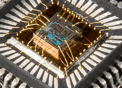
IC packaging, also known as chip packaging or semiconductor packaging, is a crucial process in the manufacturing of electronic devices. It involves encapsulating an integrated circuit (IC) chip in a protective package that allows it to be connected to other components on a printed circuit board (PCB). The primary purpose of IC packaging is to provide a means for the IC chip to interact with the outside world while protecting it from physical damage, environmental factors, and electromagnetic interference (EMI).
In this comprehensive article, we will delve into the world of IC packaging, exploring its importance, various types, and the benefits it offers to electronic devices. We will also discuss the latest trends and challenges in the IC packaging industry and answer some frequently asked questions about this essential technology.
The Importance of IC Packaging
IC packaging plays a vital role in the functioning and reliability of electronic devices. Here are some key reasons why IC packaging is essential:
Protection
One of the primary functions of IC packaging is to protect the delicate IC chip from physical damage, moisture, dust, and other environmental factors. The package acts as a barrier, shielding the chip from external hazards that could compromise its performance or cause complete failure.
Electrical Connectivity
IC packaging provides a means for the IC chip to connect to other components on the PCB. The package includes metal leads or pins that allow electrical signals to flow between the chip and the board. Without proper packaging, it would be impossible for the IC to communicate with other parts of the electronic device.
Heat Dissipation
As IC chips operate, they generate heat that must be dissipated to prevent overheating and potential damage. IC packaging often includes heat spreaders or heat sinks that help to efficiently transfer heat away from the chip, ensuring optimal performance and longevity.
Standardization
IC packaging allows for standardization in the electronic industry. By adhering to specific package types and dimensions, manufacturers can ensure compatibility between different components and simplify the design and assembly process of electronic devices.

Types of IC Packaging
There are various types of IC packaging available, each with its own advantages and applications. Some of the most common types include:
Dual In-Line Package (DIP)
DIP is one of the oldest and most widely used IC package types. It consists of a rectangular package with two parallel rows of pins extending from the sides. DIPs are commonly used in through-hole mounting applications and are favored for their ease of handling and good mechanical stability.
Small Outline Package (SOP)
SOP is a surface-mount package that offers a more compact alternative to DIP. It features a rectangular package with pins extending from two sides, allowing for higher density PCB layouts. SOPs are widely used in various electronic devices, including consumer electronics and automotive applications.
Quad Flat Package (QFP)
QFP is another surface-mount package that features pins on all four sides of the package. This arrangement allows for a higher pin count and greater connectivity options compared to SOP. QFPs are commonly used in microcontrollers, digital signal processors (DSPs), and other high-performance ICs.
Ball Grid Array (BGA)
BGA is a surface-mount package that utilizes an array of solder balls on the bottom of the package for electrical connectivity. BGAs offer a high pin count and excellent thermal and electrical performance, making them ideal for complex, high-speed applications such as graphics processors and field-programmable gate arrays (FPGAs).
Chip Scale Package (CSP)
CSP is a type of package that is only slightly larger than the IC chip itself. It offers a very compact solution for space-constrained applications, such as mobile devices and wearables. CSPs often utilize wafer-level packaging techniques, where the packaging process is performed at the wafer level before the chips are singulated.

Benefits of IC Packaging
IC packaging offers numerous benefits to electronic devices, contributing to their performance, reliability, and overall success in the market. Some of the key benefits include:
Improved Reliability
By protecting the IC chip from environmental factors and physical damage, IC packaging significantly improves the reliability of electronic devices. This increased reliability translates to longer product lifetimes, reduced failure rates, and enhanced customer satisfaction.
Enhanced Performance
IC packaging plays a crucial role in optimizing the electrical performance of electronic devices. By providing efficient electrical connectivity and minimizing signal interference, packaging technologies enable ICs to operate at higher speeds and with greater accuracy.
Miniaturization
Advances in IC packaging technologies have enabled the miniaturization of electronic devices. Smaller package sizes allow for more compact PCB layouts, enabling the development of slim, lightweight, and portable devices that are highly sought after by consumers.
Cost Reduction
IC packaging contributes to cost reduction in electronic device manufacturing. Standardized package types and sizes allow for automated assembly processes, reducing labor costs and increasing production efficiency. Additionally, advancements in packaging materials and techniques have helped to drive down the overall cost of IC packaging.

Trends and Challenges in IC Packaging
The IC packaging industry is constantly evolving to keep pace with the demands of the ever-advancing electronic device market. Some of the current trends and challenges in IC packaging include:
Advanced Packaging Technologies
As electronic devices become more sophisticated and require higher levels of performance, advanced packaging technologies are being developed to meet these demands. Examples include 2.5D and 3D packaging, which involve stacking multiple IC chips vertically or horizontally to achieve greater functionality and performance in a smaller footprint.
Heterogeneous Integration
Heterogeneous integration involves combining different types of ICs, such as processors, memory, and sensors, into a single package. This approach enables the creation of highly integrated and multifunctional electronic devices, such as system-in-package (SiP) solutions.
Thermal Management
With the increasing power densities of modern ICs, thermal management has become a critical challenge in IC packaging. Advanced packaging technologies, such as heat spreaders, thermal interface materials, and liquid cooling solutions, are being developed to effectively dissipate heat and maintain optimal device performance.
Environmental Considerations
The electronic industry is facing increasing pressure to develop environmentally friendly packaging solutions. This includes the use of lead-free and halogen-free materials, as well as the adoption of recyclable and biodegradable packaging components. The industry is also working to reduce its carbon footprint by optimizing manufacturing processes and minimizing waste.
Frequently Asked Questions (FAQ)
-
What is the difference between through-hole and surface-mount packaging?
Through-hole packaging, such as DIP, involves pins that are inserted into holes drilled in the PCB and soldered in place. Surface-mount packaging, such as SOP, QFP, and BGA, features leads or solder balls that are directly soldered onto pads on the surface of the PCB. Surface-mount packaging allows for higher component density and smaller PCB sizes. -
What is the purpose of a heat spreader in IC packaging?
A heat spreader is a component used in IC packaging to efficiently transfer heat away from the IC chip. It is typically made of a material with high thermal conductivity, such as copper or aluminum, and is placed in close contact with the chip. The heat spreader helps to distribute the heat generated by the chip over a larger surface area, facilitating better heat dissipation and preventing overheating. -
What are the advantages of using BGA packaging?
BGA packaging offers several advantages, including: - High pin count: BGAs can accommodate a large number of interconnects, making them suitable for complex ICs with numerous input/output (I/O) requirements.
- Excellent thermal and electrical performance: The solder balls in BGA packages provide low-resistance electrical paths and efficient heat transfer, enabling high-speed operation and improved thermal management.
-
Compact size: BGAs allow for high-density PCB layouts, as the solder balls are located underneath the package, saving space compared to peripheral-leaded packages.
-
What is the role of underfill in flip-chip packaging?
Underfill is a material, typically an epoxy resin, that is applied between the IC chip and the package substrate in flip-chip packaging. Its primary role is to provide mechanical support and stress relief for the solder bumps that connect the chip to the substrate. Underfill helps to distribute stress evenly, minimizing the risk of solder joint failure caused by thermal expansion mismatches between the chip and substrate materials. Additionally, underfill acts as a protective barrier, preventing moisture and contaminants from reaching the active surface of the chip. -
What are the challenges associated with package-on-package (PoP) technology?
Package-on-package (PoP) technology, which involves stacking multiple packaged ICs on top of each other, presents several challenges: - Thermal management: Stacking packages can lead to increased heat generation and difficulty in dissipating heat efficiently, requiring advanced thermal management solutions.
- Mechanical stability: The stacked structure of PoP can be prone to mechanical stress and warpage, necessitating careful design and material selection to ensure reliability.
- Signal integrity: The increased interconnect density and longer signal paths in PoP can lead to signal integrity issues, such as crosstalk and noise, requiring careful design and optimization of the package and PCB layout.
- Manufacturing complexity: PoP assembly requires precise alignment and control during the stacking process, as well as compatibility between the packages being stacked, adding complexity to the manufacturing process.
Conclusion
IC packaging is a vital aspect of electronic device manufacturing, providing protection, connectivity, and performance optimization for integrated circuits. As electronic devices continue to evolve and become more complex, the importance of advanced packaging technologies will only continue to grow. From traditional package types like DIP and SOP to cutting-edge solutions like 2.5D and 3D packaging, IC packaging plays a crucial role in enabling the development of smaller, faster, and more reliable electronic devices.
As the demand for high-performance, energy-efficient, and cost-effective electronic devices continues to rise, the IC packaging industry must adapt and innovate to meet these challenges. This includes developing new materials, processes, and design methodologies that can keep pace with the ever-increasing complexity of modern ICs.
By understanding the fundamentals of IC packaging and staying informed about the latest trends and advancements in the field, engineers, designers, and manufacturers can make informed decisions when developing and producing electronic devices. As the world becomes increasingly connected and reliant on electronics, the role of IC packaging in shaping the future of technology cannot be overstated.


Leave a Reply