Introduction to PCB Visualizer
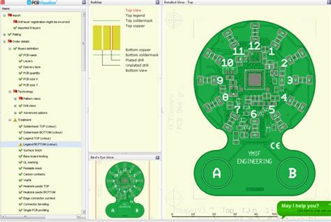
A PCB Visualizer is a software tool that allows users to view and analyze Printed Circuit Board (PCB) designs in a 3D environment. It provides a comprehensive and interactive visualization of the PCB layout, components, and connections, enabling engineers and designers to identify potential issues, optimize the design, and ensure manufacturability.
Benefits of using a PCB Visualizer
- Early detection of design flaws
- Improved collaboration among team members
- Enhanced design optimization
- Reduced time-to-market
- Cost savings through error prevention
Key Features of PCB Visualizers
3D Rendering and Navigation
PCB Visualizers offer high-quality 3D rendering of the PCB design, allowing users to view the board from various angles and zoom levels. This feature helps in understanding the spatial relationships between components, traces, and layers.
Navigation Controls
| Control | Function |
|---|---|
| Pan | Move the view horizontally or vertically |
| Rotate | Change the viewing angle of the 3D model |
| Zoom | Increase or decrease the magnification level |
Layer Visibility Control
PCB Visualizers provide the ability to selectively view or hide different layers of the PCB design. This feature is particularly useful for focusing on specific aspects of the design, such as signal integrity or power distribution.
Common PCB Layers
| Layer | Description |
|---|---|
| Top Copper | The uppermost conductive layer |
| Bottom Copper | The lowermost conductive layer |
| Inner Layers | Conductive layers sandwiched between the top and bottom layers |
| Solder Mask | Protective coating applied to the copper layers |
| Silkscreen | Text and symbols printed on the PCB surface |
Component Placement and Inspection
PCB Visualizers allow users to inspect the placement and orientation of components on the board. This feature helps in identifying potential issues related to component clearance, interference, or accessibility for assembly and maintenance.
Common Component Types
- Surface Mount Devices (SMDs)
- Through-Hole Components
- Ball Grid Arrays (BGAs)
- Connectors
- Heat Sinks
Trace Routing and Analysis
PCB Visualizers provide tools for analyzing the routing of traces on the board. Users can view the trace paths, measure distances, and check for potential signal integrity issues, such as crosstalk or impedance mismatches.
Trace Routing Considerations
- Signal Integrity
- Electromagnetic Compatibility (EMC)
- Manufacturability
- Cost Optimization
- Thermal Management
Design Rule Checking (DRC)
Many PCB Visualizers integrate Design Rule Checking (DRC) capabilities to automatically detect and highlight design violations based on predefined rules. DRC helps in ensuring that the PCB design adheres to manufacturing and electrical constraints.
Common Design Rules
- Minimum trace width and spacing
- Drill hole size and spacing
- Copper pour clearance
- Solder mask and silkscreen clearance
- Component placement and orientation

Integration with Other Tools
PCB Visualizers often integrate with other tools in the PCB design workflow, such as schematic capture software, PCB layout tools, and simulation software. This integration allows for seamless data exchange and ensures consistency throughout the design process.
Common Integrations
- Schematic Capture Software
- Altium Designer
- OrCAD Capture
- KiCad EDA
- PCB Layout Tools
- Cadence Allegro
- Mentor Graphics PADS
- Zuken CR-8000
- Simulation Software
- Ansys SIwave
- Keysight ADS
- Sigrity PowerSI

Best Practices for Using PCB Visualizers
To maximize the benefits of using a PCB Visualizer, consider the following best practices:
- Start visualizing early in the design process
- Regularly review the design with stakeholders
- Use the visualizer to communicate design intent
- Leverage the visualizer for design optimization
- Integrate the visualizer into the design workflow

Case Studies
Case Study 1: Automotive ECU Design
An automotive electronics manufacturer used a PCB Visualizer to design a complex Engine Control Unit (ECU). The visualizer helped the team identify and resolve signal integrity issues, optimize component placement for thermal management, and ensure compliance with automotive design standards. As a result, the company reduced the design cycle time by 25% and improved the overall reliability of the ECU.
Case Study 2: Medical Device Development
A medical device company employed a PCB Visualizer to develop a compact, high-density PCB for a wearable health monitoring device. The visualizer allowed the design team to optimize the layout for manufacturability, minimize the device size, and ensure proper shielding for electromagnetic compatibility (EMC). By using the visualizer, the company accelerated the development process and successfully launched the product on time, meeting all regulatory requirements.
Future Trends in PCB Visualization
As PCB designs continue to increase in complexity and density, the role of PCB Visualizers will become even more critical. Some of the future trends in PCB visualization include:
- Integration of Augmented Reality (AR) and Virtual Reality (VR) technologies
- Incorporation of Artificial Intelligence (AI) for design optimization and error detection
- Cloud-based collaboration and visualization platforms
- Real-time simulation and analysis within the visualizer environment
- Seamless integration with additive manufacturing processes
Conclusion
PCB Visualizers have become an indispensable tool for engineers and designers involved in the development of electronic products. By providing a comprehensive and interactive 3D view of the PCB design, visualizers enable early detection of design flaws, facilitate collaboration, and optimize the design for manufacturability and performance. As the complexity of PCB designs continues to grow, the adoption of advanced visualization techniques will be crucial for staying competitive in the industry.
Frequently Asked Questions (FAQ)
1. What are the system requirements for running a PCB Visualizer?
The system requirements for running a PCB Visualizer vary depending on the specific software and the complexity of the PCB design. Generally, a modern computer with a multi-core processor, dedicated graphics card, and sufficient RAM (8 GB or more) is recommended for optimal performance.
2. Can PCB Visualizers import designs from different PCB layout tools?
Yes, most PCB Visualizers support importing design files from various PCB layout tools, such as Altium Designer, Cadence Allegro, and Mentor Graphics PADS. However, it is essential to check the specific file formats supported by the visualizer software.
3. Are there any open-source or free PCB Visualizers available?
While many commercial PCB Visualizers offer advanced features and integrations, there are also open-source and free alternatives available. Some popular open-source options include KiCad’s 3D Viewer and FreeCAD’s PCB Workbench. These tools may have limited functionality compared to commercial solutions but can still be useful for basic visualization needs.
4. How can I collaborate with my team using a PCB Visualizer?
Many PCB Visualizers offer collaboration features, such as cloud-based sharing, real-time updates, and version control. These features allow team members to access and review the PCB design simultaneously, provide feedback, and make changes in a collaborative environment.
5. Can PCB Visualizers simulate the operation of the PCB?
Some advanced PCB Visualizers integrate with simulation software to provide real-time simulation capabilities within the visualization environment. This allows users to analyze the electrical and thermal behavior of the PCB under various operating conditions. However, the availability and extent of simulation features may vary depending on the specific visualizer software.


Leave a Reply