What are Rigid PCBs?
A printed circuit board (PCB) is a thin board made of fiberglass or other insulating material used to mechanically support and electrically connect electronic components using conductive tracks, pads and other features. Rigid PCBs are the most common type of PCBs and provide a sturdy base for mounting and interconnecting electronic components.
Rigid PCBs get their name from the fact that they retain their shape and do not flex. The rigid fiberglass material allows components to be densely packed onto the board without flexing. This makes rigid PCBs suitable for products that do not require flexibility such as computers, appliances, instruments and automotive electronics.
Features of Rigid PCBs
- Made of rigid insulating material like FR-4 fiberglass
- Retains shape and does not flex
- Allows for dense component packing
- Most common and cost-effective PCB type
- Suitable for high volume production
- Used in products not requiring flexibility
Some key properties and advantages of rigid PCBs:
- Strong and durable – The rigid fiberglass material is mechanically strong and can withstand vibration, shock and temperature fluctuations.
- Heat resistance – Rigid PCBs can operate at high temperatures of over 100°C making them suitable for power electronic applications.
- Dimensional stability – They retain their shape and size which allows for accurate component spacing and routing.
- Design freedom – Rigid boards allow greater component density and more routing layers due to their stability.
- Easy assembly – Components can be easily soldered onto rigid PCBs using wave or reflow soldering techniques.
- Cost effective – Rigid PCB fabrication methods are very efficient resulting in lower costs compared to flexible PCBs.
Rigid PCB Materials
The most common materials used to fabricate the rigid insulating substrate for PCBs are:
- FR-4 Glass Epoxy – The most popular and inexpensive material composed of woven fiberglass cloth with an epoxy resin binder. Different grades are available with temperature ratings from 130°C to over 170°C.
- CEM-1 Cotton Paper – Made of pressed cotton paper with epoxy resin. It has good mechanical strength and allows small hole drilling but lower temperature rating.
- FR-5 Glass Epoxy – Woven fiberglass reinforced epoxy with very high temperature rating over 170°C suitable for high power applications. More expensive than FR-4.
- Polymide – A high temperature resistant synthetic polymer film used for rigid-flex PCBs requiring stable material performance.
- Aluminum – Rigid aluminum PCBs provide excellent thermal conductivity and electromagnetic shielding. Mainly used for LED lighting and power electronics.
Rigid PCB Construction
Rigid PCBs are built up with layers of conductive copper and insulating dielectric material to create a multilayer board with complex interconnections. Here are the main construction elements:
- Substrate – The base insulating layer providing mechanical support is typically 0.4mm to 2mm thick FR-4 fiberglass.
- Copper layers – The conductive layers are made from thin copper foil laminated onto the substrate. There may be 1 to over 30 layers.
- Dielectric layers – Additional sheets of rigid insulating material like FR-4 are stacked between copper layers as needed to create multilayer PCBs.
- Vias – Hollow copper plated through holes that provide vertical interconnection between copper layers.
- Finish – The outer copper layers are coated with solder mask and silkscreen for protection and component labeling.
- Edge plating – Copper plating along the edges of the PCB to facilitate electrical connections between layers.
- Solder mask – Epoxy based layer over the outer copper layers with openings for soldering components. Prevents solder bridging.
- Silkscreen – White epoxy ink layer for marking component designators, logos and board text.
Rigid PCB Design Principles
Designing a rigid PCB requires careful planning and layout to create a functional board that can be easily manufactured. Here are some key rigid PCB design guidelines:
Component Placement
- Place components for shortest routing between connections
- Group associated components together
- Ensure adequate spacing between components for heat dissipation and manufacturing
- Place sensitive components away from noise sources
- Optimize placement for manufacturing ease and testability
Routing and Traces
- Use 45° and 90° angles for traces
- Use minimum trace widths based on current flow
- Minimize vias and crossed traces while routing
- Avoid 90° bends on high speed traces
- Match trace lengths for critical signals like clocks
- Provide proper clearances between traces and pads
Layer Stackup
- Assign power and ground planes adjacent to outer layers
- Use thicker copper weights for power distribution layers
- Add layer pairs to isolate critical signals
- Minimize layer counts to reduce cost
Board Shape and Size
- Make board compact while allowing access for test points
- Allow margin on edges for manufacturing tolerance
- Include tooling holes for assembly fixtures
- Follow fabrication panel sizes or allow breaking tabs
Fabrication and Assembly
- Choose surface finish suitable for soldering method
- Specify soldermask openings for ease of soldering
- Mark component locations with polarized silkscreen symbols
- Provide testpoints to access internal circuit nodes
- Follow assembly guidelines for component spacing
By following these design practices, a rigid PCB can be optimized for manufacture and performance.
Rigid PCB Manufacturing Process
Rigid PCBs go through an intricate fabrication process to create the layered board with etched copper traces. Here are the key manufacturing steps:
1. Inner Layer Production
- Start with bare copper clad rigid substrate
- Image photoresist pattern for traces using lithography
- Etch away unwanted copper to leave behind traced circuitry
- Strip off remaining photoresist
2. Layer Stackup
- Arrange inner layer cores alternated with prepreg bonding sheets
- Align layers using tooling holes
- Laminate under heat and pressure to bond layers into a board
3. Through Hole Drilling
- Drill holes through the multilayer board for vias
- Use smaller bits for component holes followed by larger bits for vias
- Ensure drill alignment between layers
4. Hole Plating
- Plate conductive copper along the interior of drilled holes
- Electroless plating deposits initial copper layer
- Electroplating grows copper thickness to required extent
5. Outer Layer Imaging
- Coat outer layers with photoresist and expose image of traces
- Remove unexposed areas to create desired conductor pattern
6. Soldermask Application
- Layer of epoxy soldermask applied over entire board
- Portions exposed over solder pads and connectors
7. Silkscreen Printing
- Print white epoxy ink markings through patterned screens
- Indicates component designators, polarity markings etc
8. Surface Finish
- Coat exposed copper with solder, gold or other surface finish
- Used for protection against oxidation and improved solderability
9. Routing
- Cut boards from panel into individual PCBs
- May involve v-scoring or punching depending on volume
10. Electrical Testing
- Test for shorts, opens and proper functioning
- Checks for damage during fabrication and assembly
This multi-step process transforms raw PCB materials into complex, multilayer printed circuit boards ready for component assembly.
Types of Rigid PCBs
There are several specific types of rigid PCBs designed for specialized applications:
Single Sided PCBs
The simplest PCBs with copper traces on only one side of the substrate. Lower component density but lowest cost.
Double Sided PCBs
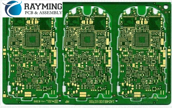
Copper layers on both sides of the PCB allow increased wiring density. Most common rigid PCB type.
Multilayer PCBs
Have 3 or more conductive layers separated by dielectric material. Allows complex interconnections.
High Frequency PCBs
Designed for high speed signals and radio frequencies. Use controlled impedances and isolation.
High Power PCBs
Handle large currents and heat loads. Use thick copper layers for power distribution.
Metal Core PCBs
Insulated metal base provides thermal and structural support. Used for LEDs and power devices.
Thick Copper PCBs
Utilize copper thickness up to 400um for very high current capacity. Prevent overheating.
HDI PCBs
Have higher trace densities and thin dielectrics. Accommodate finepitch components.
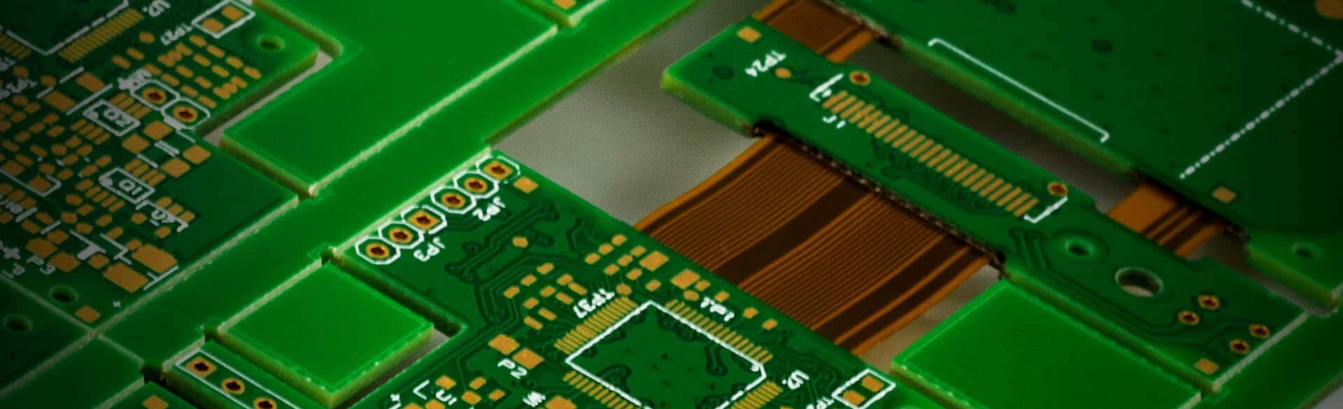
Rigid-Flex PCBs
Combine rigid and flexible sections for complex interconnections. Fold into 3D shapes.
There are many types of rigid PCBs tailored for the specific design requirements.
Applications of Rigid PCBs
Due to their beneficial properties, performance and cost-effectiveness, rigid PCBs are used in countless electronic devices:
Computers and Servers
The core circuit boards in computers with processors, memory and expansion slots are made of rigid PCBs. High layer counts accommodate complex circuitry.
Consumer Electronics
Appliances, gadgets and home electronics widely use double sided and multilayer rigid boards for the control circuitry.
Automobiles
Many ECUs and electronics modules governing modern engine and body systems rely on rigid boards. Withstand harsh environments.
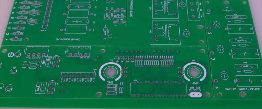
Industrial Electronics
Instruments, programmable logic controllers and motor drives in factories have embedded rigid PCBs to operate reliably for years.
Medical Equipment
Rigid boards provide the robust foundation for the sensitive and critical electronics used in medical diagnostic systems.
Telecommunications
Networking gear with switches, routers and base stations contains high speed rigid PCBs for data transmission.
Military/Aerospace
Avionics systems with flight controls and weapons systems utilize specialized rigid boards that meet stringent quality standards.
The unmatched versatility of rigid PCBs makes them indispensable across every electronics sector.
Comparison of Rigid and Flexible PCBs
While rigid PCBs are ideal for many applications, flexible PCBs have advantages in certain situations. Here is a comparison between rigid and flex PCB characteristics:
| Parameter | Rigid PCB | Flexible PCB |
|---|---|---|
| Composition | Rigid fiberglass substrate | Thin polymer film substrate |
| Layer Types | Copper conductor layers | Copper or conductive ink |
| Geometry | Flat, fixed shape | Can flex and bend |
| Component Density | Very High | Moderate |
| Routing Density | Many routing layers | 1-2 layers typical |
| Design Complexity | Very complex, high layer counts | Simpler, fewer layers |
| Applications | Ideal for complex circuitry in fixed structures | Used where flexibility needed |
| Cost | Lower cost due to high production efficiency | Typically higher cost |
| Manufacturability | Mature processes, highly optimized | Challenging thin materials require tighter process controls |
| Lead time | Standard ~2-4 week lead times | Often longer lead times around 4-6 weeks |
| Reliability | Very reliable with high MTBF | Flexing can stress materials reducing reliability |
In summary, rigid PCBs are the workhorse of the industry while flex PCBs meet specialized requirements for flexible assemblies and interconnections.
Rigid PCB Design Software
To efficiently design modern rigid PCBs, engineers use electronic design automation (EDA) software for schematic capture and PCB layout. These tools allow faster design with more reliable outcomes. Here are some leading rigid PCB design software options:
Altium Designer
Altium is one of the most full-featured and widely used PCB design platforms. It integrates schematic capture, 3D modeling and PCB layout in a unified environment. Advanced capabilities for high speed, high power and multilayer boards.
Cadence Allegro
Allegro offers a powerful PCB design ecosystem with tools for planning, layout, analysis and manufacturing. Used for many complex, mission-critical PCB designs.
Mentor Graphics Xpedition
Trusted tools from Mentor for the complete PCB workflow including layout, high speed design and manufacturability checks.
Zuken CR-8000
The CR-8000 promises faster rigid PCB design with its adaptive routing and shaping algorithms to optimize layout.
Solidworks PCB
This CAD-centric tool allows PCB design integrated with 3D modeling for collaboration between electrical and mechanical teams.
With continual improvements in software capabilities, productivity in rigid PCB design continues to accelerate.
Rigid PCB Manufacturers
There are thousands of PCB manufacturers around the world that offer rigid PCB fabrication and assembly services. Here are some of the leading global rigid PCB manufacturers:
- TTM Technologies
- AT&S
- Tripod Technology
- Unimicron
- Ibiden
- Zhen Ding Tech
- Shennan Circuits
- Kinwong
- Multek
- WUS Printed Circuit
- Shenzhen Fastprint
Many of these companies operate large scale highly automated manufacturing facilities and offer the complete range of rigid, flex, metal core and HDI PCBs. They provide essential capacity for the huge global demand for rigid PCBs across all industries.
Factors to evaluate when selecting a rigid PCB supplier include:
- Technical capabilities – number of layers, trace/space, via structures etc
- Certifications – ISO, automotive, aerospace, ITAR etc
- Production capacity – volume requirements
- Location – impact on logistics and lead time
- First article sample turn time
- Communication and customer support
- Pricing and minimum order quantity
FQA about Rigid PCBs
What are some other names for a rigid PCB?
Rigid PCBs are also known as:
- FR4 boards
- Glass epoxy boards
- Composites boards
- Circuit boards
- Printed wiring boards (PWBs)
What are the dimensions of a typical rigid PCB?
Rigid PCB sizes can range from under 1 inch square to over 3 feet on each edge. Typical dimensions are:
- Length – 100 to 250 mm
- Width – 100 to 250 mm
- Thickness – 0.4 to 6 mm
What are the key thermal properties of FR4 material used in rigid PCBs?
- Glass transition temperature (Tg) – 130 to 180°C
- Coefficient of thermal expansion (CTE) – 14 to 20 ppm/°C
- Thermal conductivity – 0.25 to 0.35 W/mK
What is the typical temperature rating for a multilayer FR4 PCB?
The maximum rated temperature for common FR4 and 106 laminates is 130°C. High Tg variants can operate up to 180°C.
What is the typical copper thickness used on outer layers of rigid PCBs?
A common used standard copper thickness for rigid PCB outerlayers is 1 oz copper which corresponds to around 35 microns. Thicker 2 oz (70 um) copper may be used for high current applications.
What are the standard thickness values for FR4 based rigid PCB dielectric substrates?
Common FR4 substrate thickness values are:
- 0.4 mm
- 0.6 mm
- 0.8 mm
- 1.0 mm
- 1.2 mm
- 1.6 mm
- 2.0 mm
Thicker substrates over 3mm are also possible but less common.
Conclusion
Rigid printed circuit boards remain the backbone of electronics due to their reliable performance, design flexibility and manufacturability. Continual technology improvements allow more layers, higher densities and advanced materials to meet increasing demands. With their unmatched versatility to support everything from consumer gadgets to advanced robotics, the role of rigid PCBs will remain indispensable for the foreseeable future across the entire electronics industry.


Leave a Reply