Introduction to PCB Panel Optimization
Printed Circuit Board (PCB) manufacturing is a complex process that involves multiple steps, from design to fabrication. One of the most critical aspects of PCB manufacturing is panel utilization, which refers to the efficient use of the available space on a PCB panel. Optimizing panel utilization can lead to significant cost savings, reduced material waste, and improved production efficiency.
In this article, we will explore the concept of PCB panel optimization, its importance, and various techniques to achieve optimal panel utilization. We will also discuss the factors that influence panel utilization and how to overcome common challenges in the process.
What is PCB Panel Optimization?
PCB panel optimization is the process of maximizing the number of PCBs that can be manufactured on a single panel while minimizing material waste and production costs. A PCB panel is a large sheet of material, typically made of FR-4 or other substrates, on which multiple PCBs are fabricated simultaneously.
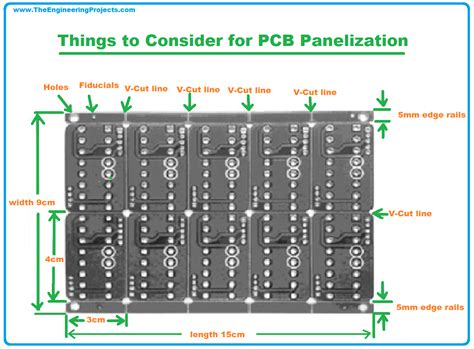
The goal of panel optimization is to arrange the PCBs on the panel in a way that maximizes the use of available space while ensuring that the PCBs meet the required specifications and quality standards. This involves considering various factors such as PCB size, shape, orientation, spacing, and tooling holes.

Importance of PCB Panel Optimization
PCB panel optimization is crucial for several reasons:
-
Cost Savings: Optimizing panel utilization can lead to significant cost savings by reducing material waste and increasing the number of PCBs produced per panel. This, in turn, lowers the cost per PCB and improves overall profitability.
-
Increased Production Efficiency: By maximizing the number of PCBs per panel, manufacturers can reduce the number of panels required to fulfill an order, thereby increasing production efficiency and reducing lead times.
-
Reduced Environmental Impact: Optimizing panel utilization helps minimize material waste, which is beneficial for the environment. This is particularly important considering the increasing focus on sustainable manufacturing practices.
-
Improved Quality: Proper panel optimization ensures that PCBs are fabricated with the required spacing and tooling holes, which helps maintain the quality and reliability of the final product.

Factors Influencing PCB Panel Utilization
Several factors influence PCB panel utilization, including:
-
PCB Size and Shape: The size and shape of the PCBs play a crucial role in determining panel utilization. Smaller and more uniformly shaped PCBs allow for better panel utilization compared to larger and irregularly shaped ones.
-
Panelization Scheme: The panelization scheme refers to the arrangement of PCBs on the panel. Different panelization schemes, such as grid, step-and-repeat, or custom panelization, can impact panel utilization.
-
Spacing and Tooling Holes: The spacing between PCBs and the placement of tooling holes can affect panel utilization. Adequate spacing is necessary to ensure proper singulation and to avoid damage during the depaneling process.
-
Material Selection: The choice of material, such as FR-4 or aluminum-backed PCBs, can influence panel utilization. Different materials have varying properties and manufacturing constraints that must be considered during panel optimization.
-
Manufacturing Capabilities: The manufacturing capabilities of the PCB fabricator, such as minimum feature sizes, layer counts, and available panel sizes, can impact panel utilization.

Techniques for PCB Panel Optimization
There are several techniques that can be used to optimize PCB panel utilization:
-
Panelization Software: Panelization software tools automate the process of arranging PCBs on a panel. These tools consider various factors such as PCB size, shape, spacing, and tooling holes to generate optimal panelization layouts.
-
Design for Manufacturability (DFM): Incorporating DFM principles during the PCB design phase can help optimize panel utilization. This includes designing PCBs with standardized sizes and shapes, minimizing irregular features, and following recommended spacing and tooling hole guidelines.
-
Multi-PCB Panelization: Multi-PCB panelization involves combining multiple different PCB designs on a single panel. This technique can help maximize panel utilization, especially when dealing with low-volume production runs or prototypes.
-
Nested Panelization: Nested panelization is a technique where smaller PCBs are placed within the cutouts of larger PCBs to maximize panel utilization. This method is particularly useful when dealing with a mix of PCB sizes and shapes.
-
Custom Panelization: In some cases, custom panelization may be necessary to achieve optimal panel utilization. This involves creating a unique panelization layout that takes into account the specific requirements of the PCB design and manufacturing process.
Challenges in PCB Panel Optimization
Despite the benefits of PCB panel optimization, there are several challenges that manufacturers may face:
-
Complex PCB Designs: PCBs with complex shapes, irregular features, or varying sizes can pose challenges for panel optimization. These designs may require custom panelization or specialized manufacturing techniques.
-
Manufacturing Constraints: Manufacturing constraints, such as minimum feature sizes, layer counts, and available panel sizes, can limit the options for panel optimization. Manufacturers must work within these constraints to achieve the best possible panel utilization.
-
Material Availability: The availability of specific materials, such as high-performance substrates or specialized laminates, can impact panel optimization. Manufacturers may need to adjust their panelization strategies based on material availability and lead times.
-
Cost Considerations: While panel optimization can lead to cost savings, it may also involve additional costs, such as the need for specialized software tools or custom manufacturing processes. Manufacturers must balance the cost benefits of panel optimization with the associated expenses.
Best Practices for PCB Panel Optimization
To achieve optimal PCB panel utilization, manufacturers should follow these best practices:
-
Collaborate with PCB Designers: Encourage collaboration between PCB designers and manufacturing engineers to ensure that PCB designs are optimized for manufacturability and panel utilization.
-
Standardize PCB Sizes and Shapes: Where possible, standardize PCB sizes and shapes to facilitate easier panelization and improve panel utilization.
-
Use Panelization Software: Invest in panelization software tools to automate the process of arranging PCBs on a panel and generate optimal panelization layouts.
-
Follow DFM Guidelines: Ensure that PCB designs follow DFM guidelines, including recommended spacing, tooling hole placement, and minimum feature sizes.
-
Consider Multi-PCB and Nested Panelization: Explore the use of multi-PCB and nested panelization techniques to maximize panel utilization, especially for low-volume production runs or prototypes.
-
Monitor and Analyze Panel Utilization: Regularly monitor and analyze panel utilization metrics to identify areas for improvement and optimize the panelization process continuously.
Conclusion
PCB panel optimization is a critical aspect of PCB manufacturing that can lead to significant cost savings, improved production efficiency, and reduced environmental impact. By understanding the factors that influence panel utilization and employing various optimization techniques, manufacturers can maximize the number of PCBs produced per panel while minimizing material waste.
To achieve optimal panel utilization, manufacturers must collaborate with PCB designers, follow DFM guidelines, invest in panelization software, and explore advanced techniques such as multi-PCB and nested panelization. By continuously monitoring and analyzing panel utilization metrics, manufacturers can identify areas for improvement and refine their panelization strategies over time.
As the demand for high-quality, cost-effective PCBs continues to grow, the importance of PCB panel optimization cannot be overstated. By prioritizing panel optimization, PCB manufacturers can remain competitive in an increasingly challenging market while contributing to a more sustainable future.
Frequently Asked Questions (FAQ)
1. What is the difference between panelization and PCB panel optimization?
Panelization refers to the process of arranging multiple PCBs on a single panel for fabrication. PCB panel optimization, on the other hand, is the process of maximizing the number of PCBs that can be placed on a panel while minimizing material waste and ensuring that the PCBs meet the required specifications and quality standards.
2. How does PCB panel optimization impact the cost of PCB manufacturing?
PCB panel optimization can significantly reduce the cost of PCB manufacturing by minimizing material waste and increasing the number of PCBs produced per panel. This leads to lower cost per PCB and improved overall profitability for the manufacturer.
3. What are some common techniques used for PCB panel optimization?
Some common techniques used for PCB panel optimization include the use of panelization software, multi-PCB panelization, nested panelization, and custom panelization. These techniques help maximize panel utilization by considering factors such as PCB size, shape, spacing, and tooling holes.
4. How can PCB designers contribute to panel optimization?
PCB designers can contribute to panel optimization by following Design for Manufacturability (DFM) guidelines, which include designing PCBs with standardized sizes and shapes, minimizing irregular features, and adhering to recommended spacing and tooling hole guidelines. Collaboration between PCB designers and manufacturing engineers is crucial for achieving optimal panel utilization.
5. What are some challenges faced by manufacturers in PCB panel optimization?
Some challenges faced by manufacturers in PCB panel optimization include dealing with complex PCB designs, working within manufacturing constraints such as minimum feature sizes and available panel sizes, material availability, and balancing the cost benefits of panel optimization with associated expenses such as specialized software tools or custom manufacturing processes.
| Factor | Impact on Panel Utilization |
|---|---|
| PCB Size and Shape | Smaller and more uniform PCBs allow for better utilization compared to larger and irregular ones |
| Panelization Scheme | Different schemes (grid, step-and-repeat, custom) can impact utilization |
| Spacing and Tooling Holes | Adequate spacing and proper tooling hole placement are necessary for optimal utilization |
| Material Selection | Different materials have varying properties and constraints that affect utilization |
| Manufacturing Capabilities | Minimum feature sizes, layer counts, and available panel sizes impact utilization |
Table 1: Factors influencing PCB panel utilization and their impact.
By considering these factors and employing the techniques and best practices discussed in this article, PCB manufacturers can optimize their panel utilization, leading to cost savings, improved efficiency, and a more sustainable manufacturing process.


Leave a Reply