Introduction to PCB Layers
Printed Circuit Boards (PCBs) are essential components in modern electronics, providing a platform for mounting and interconnecting electronic components. One of the key aspects of PCB design is the number and arrangement of layers within the board. In this comprehensive guide, we will delve into the world of PCB layers, answering frequently asked questions and providing insights to help you understand and optimize your PCB designs.
What are PCB Layers?
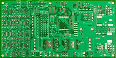
PCB layers are the individual layers of copper and insulating material that make up a printed circuit board. These layers work together to provide electrical connections and insulation between components on the board. The number of layers in a PCB can vary depending on the complexity and requirements of the circuit design.
Why are PCB Layers Important?
PCB layers play a crucial role in the functionality, reliability, and performance of electronic devices. They enable the routing of signals, power, and ground connections between components, while also providing mechanical support and protection. The proper selection and arrangement of PCB layers can significantly impact the following aspects:
- Signal Integrity
- Power Distribution
- Electromagnetic Compatibility (EMC)
- Thermal Management
- Manufacturing Feasibility and Cost
Types of PCB Layers
PCBs can be classified based on the number of layers they contain. Let’s explore the common types of PCB layers:
Single Layer PCBs
Single layer PCBs, also known as single-sided PCBs, have copper traces on only one side of the board. The components are mounted on the same side as the copper traces. These PCBs are the simplest and most cost-effective option, suitable for basic circuits with low component density.
Double Layer PCBs
Double layer PCBs, or double-sided PCBs, have copper traces on both sides of the board. Components can be mounted on either side, and the two layers are connected using through-hole vias. Double layer PCBs offer increased routing flexibility and higher component density compared to single layer PCBs.
Multi-Layer PCBs
Multi-layer PCBs consist of three or more layers of copper, separated by insulating material. The layers are interconnected using vias, allowing for complex routing and higher component density. Common multi-layer configurations include:
- 4-Layer PCBs
- 6-Layer PCBs
- 8-Layer PCBs
- 10-layer PCBs and beyond
Multi-layer PCBs are used in advanced electronic systems that require high-speed signaling, dense component packaging, and improved EMC performance.

PCB Layer Stack-up
The arrangement of layers in a PCB is known as the layer stack-up. It defines the order and purpose of each layer in the board. A typical PCB layer stack-up consists of the following layers:
- Top Layer (Signal Layer)
- Ground Layer
- Power Layer
- Signal Layers (Inner Layers)
- Bottom Layer (Signal Layer)
The number and arrangement of layers in the stack-up depend on the specific design requirements, such as signal integrity, power distribution, and EMC considerations.
Signal Layers
Signal layers are used for routing the electrical signals between components on the PCB. They are typically located on the outer layers (top and bottom) and inner layers of the board. The placement and routing of signals on these layers are critical for maintaining signal integrity and minimizing crosstalk.
Power and Ground Layers
Power and ground layers are dedicated to distributing power and providing a low-impedance return path for signals. They are usually placed adjacent to each other in the layer stack-up to form a power plane and a ground plane. The power and ground planes help to minimize impedance, reduce noise, and improve EMC performance.
Insulating Layers
Insulating layers, also known as dielectric layers, provide electrical isolation between the conductive layers in the PCB. They are typically made of materials such as FR-4, which is a glass-reinforced epoxy laminate. The thickness and properties of the insulating layers affect the impedance and signal propagation characteristics of the PCB.

Designing with PCB Layers
When designing a PCB, it’s essential to consider the number and arrangement of layers based on the specific requirements of your project. Here are some key factors to keep in mind:
Signal Integrity
Signal integrity refers to the ability of a signal to maintain its intended characteristics as it propagates through the PCB. To ensure good signal integrity, consider the following:
- Use appropriate trace widths and spacing based on the signal frequencies and impedance requirements.
- Minimize the length of high-speed signal traces to reduce reflections and crosstalk.
- Use proper termination techniques, such as series termination or parallel termination, to match the impedance of the traces.
- Separate sensitive signals from noisy signals by using different layers or providing adequate spacing.
Power Distribution
Efficient power distribution is crucial for the reliable operation of the PCB. Consider the following guidelines:
- Use dedicated power and ground layers to provide low-impedance power distribution.
- Place power and ground planes close to each other to form a high-frequency capacitor, reducing power supply noise.
- Use appropriate via sizes and placement to minimize voltage drop and improve current carrying capacity.
- Decouple power supplies using capacitors placed close to the power pins of components.
Electromagnetic Compatibility (EMC)
EMC refers to the ability of an electronic device to operate without causing or being affected by electromagnetic interference. To improve EMC performance:
- Use ground planes to provide a low-impedance return path for high-frequency signals.
- Implement proper grounding techniques, such as star grounding or hybrid grounding, to minimize ground loops and noise coupling.
- Use shielding techniques, such as copper pours or shielding cans, to contain electromagnetic radiation.
- Follow guidelines for trace routing, such as avoiding sharp bends and minimizing loop areas, to reduce electromagnetic emissions.
Thermal Management
Proper thermal management is essential to ensure the reliability and longevity of the PCB. Consider the following:
- Use appropriate copper weights and trace widths to handle the expected current levels without excessive heating.
- Provide sufficient spacing between power-dissipating components to allow for heat dissipation.
- Use thermal vias to transfer heat from components to other layers or to an external heatsink.
- Consider using thermal management techniques, such as copper pours or thermal interface materials, to improve heat dissipation.

FAQ
1. How do I determine the number of layers needed for my PCB?
The number of layers required for your PCB depends on several factors, including:
- The complexity of the circuit design
- The number and type of components
- The signal integrity and power distribution requirements
- The available board space and form factor
As a general guideline, simple circuits with low component density can often be implemented using single or double layer PCBs. More complex designs with high-speed signals, dense component placement, and strict EMC requirements may require multi-layer PCBs with four or more layers.
It’s essential to consider the trade-offs between the number of layers and factors such as manufacturing cost, board thickness, and design complexity. Consult with your PCB manufacturer or an experienced PCB designer to determine the optimal number of layers for your specific project.
2. Can I mix different types of signals on the same layer?
While it is possible to route different types of signals on the same layer, it is generally recommended to separate them to minimize crosstalk and signal integrity issues. Here are some guidelines:
- Route high-speed signals on dedicated layers, away from lower-speed signals and power traces.
- Separate analog and digital signals to prevent noise coupling.
- Use ground planes or guard traces to isolate sensitive signals from potential sources of interference.
If mixing signals on the same layer is unavoidable due to board space constraints, ensure adequate spacing between the traces and consider using techniques such as differential signaling or shielding to minimize crosstalk.
3. How do I choose the right layer stack-up for my PCB?
Choosing the right layer stack-up depends on the specific requirements of your design. Consider the following factors:
- Signal integrity: Determine the number and placement of signal layers based on the signal speeds, trace lengths, and routing density.
- Power distribution: Allocate dedicated power and ground layers to provide low-impedance power distribution and minimize noise.
- EMC: Use ground planes and proper grounding techniques to improve EMC performance.
- Manufacturing constraints: Consider the capabilities and limitations of your PCB manufacturer, such as the minimum layer count, layer spacing, and via sizes.
Collaborate with your PCB manufacturer and consider industry-standard layer stack-ups for your specific application. They can provide guidance on the optimal layer arrangement and materials based on your design requirements.
4. What are blind and buried vias, and when should I use them?
Blind and buried vias are specialized types of vias used in multi-layer PCBs:
- Blind vias: These vias start from an outer layer and terminate on an inner layer, without reaching the opposite side of the board.
- Buried vias: These vias connect inner layers without reaching either of the outer layers.
Blind and buried vias are used in advanced PCB designs to achieve higher routing density, improve signal integrity, and reduce board size. They allow for more efficient use of board space by freeing up routing channels on the outer layers.
However, blind and buried vias come with additional manufacturing complexity and cost compared to through-hole vias. They require specialized manufacturing processes and may have limitations on the minimum via size and depth.
Consider using blind and buried vias when:
- Board space is limited, and high routing density is required.
- Signal integrity is critical, and shorter via lengths are needed to minimize signal reflections.
- The design requires a high degree of layer-to-layer connectivity.
Consult with your PCB manufacturer to determine the feasibility and cost implications of using blind and buried vias in your design.
5. How do I ensure proper impedance control in my PCB design?
Impedance control is crucial for maintaining signal integrity, especially in high-speed designs. Here are some tips to ensure proper impedance control:
- Choose appropriate trace widths and spacing based on the desired impedance and the dielectric properties of the PCB material.
- Use a consistent dielectric thickness between the signal layer and the reference plane (ground or power).
- Maintain a continuous reference plane beneath the signal traces to provide a stable return path.
- Avoid abrupt changes in trace width or direction, which can cause impedance discontinuities.
- Use impedance-controlled vias, such as back-drilled or blind vias, to minimize impedance mismatches.
- Perform impedance simulations and measurements to verify the impedance of critical traces.
Consult with your PCB manufacturer or use impedance calculation tools to determine the appropriate trace geometries and layer stack-up for your desired impedance.
Conclusion
Understanding PCB layers is essential for designing reliable, high-performance electronic systems. By carefully considering the number and arrangement of layers, you can optimize signal integrity, power distribution, EMC, and thermal management in your PCB designs.
Remember to collaborate with your PCB manufacturer and follow industry guidelines and best practices when designing your layer stack-up. By doing so, you can ensure that your PCB meets the specific requirements of your application and achieves optimal performance and reliability.
As technology advances and electronic systems become more complex, the importance of effective PCB layer design will only continue to grow. By staying informed and adapting to new techniques and materials, you can stay ahead of the curve and create PCBs that push the boundaries of innovation.
| PCB Type | Number of Layers | Typical Applications |
|---|---|---|
| Single Layer PCB | 1 | Simple, low-density circuits |
| Double Layer PCB | 2 | Medium complexity circuits, general purpose |
| 4-Layer PCB | 4 | Complex digital and mixed-signal circuits |
| 6-Layer PCB | 6 | High-speed digital and RF circuits |
| 8-Layer PCB | 8 | Advanced high-speed and dense circuits |
| 10+ Layer PCB | 10 or more | Highly complex, high-performance systems |
Table 1: Common PCB layer configurations and their typical applications.
| Layer Type | Purpose |
|---|---|
| Signal Layer | Routing electrical signals between components |
| Power Layer | Distributing power to components, providing low-impedance path |
| Ground Layer | Providing reference plane and return path for signals |
| Insulating Layer | Providing electrical isolation between conductive layers |
Table 2: Types of layers in a PCB and their purposes.
By understanding the roles and characteristics of different PCB layers, you can make informed decisions when designing your PCBs and ensure that they meet the performance, reliability, and cost requirements of your projects.
Happy PCB designing!


Leave a Reply