What is a PCB?
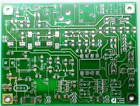
A PCB, or printed circuit board, is the foundation of nearly all modern electronic devices. PCBs are flat boards made of insulating materials like fiberglass, with conductive copper traces printed onto the surface in a specific pattern. Electronic components like resistors, capacitors, and integrated circuits are then soldered onto the board to create a complete circuit.
PCBs allow circuits to be mass produced in a standardized way. They mechanically support and electrically connect all the components using conductive pathways etched from copper sheets laminated onto a non-conductive substrate. PCBs can be single-sided (one copper layer), double-sided (two copper layers), or multi-layered (outer and inner layers).
Advantages of PCBs
PCBs offer many advantages over other types of circuits:
- Compact size
- Low electronic noise
- Reduced wiring
- Easy to mass produce
- Reliable and durable
- Lower assembly costs
PCB Composition
A typical PCB consists of several different layers:
| Layer | Description |
|---|---|
| Silkscreen | The white text and symbols printed on the PCB that identify components and test points. Does not carry any current. |
| Soldermask | The green coating that covers the copper traces. Prevents accidental contact with other metal, solder, or conductive parts. |
| Copper | Thin layers of copper foil laminated onto the substrate. Etched into the distinctive patterns of PCB traces, pads, and vias. |
| Substrate | The insulating foundation that supports the copper layers, usually FR4 fiberglass. |
Additional layers may include:
- Solder paste layers
- Solder mask layers
- Nomenclature layers
- Drill layers
- Extra copper layers for complex designs

PCB Design Flow
The PCB design process typically follows these steps:
-
Schematic capture – Creating the symbolic representation of the circuit in a schematic editor like EDA.
-
Component placement – Arranging the components on the board for optimal routing and functionality.
-
Routing traces – Drawing copper traces to connect component pins according to the schematic.
-
DRC (Design Rule Check) – Automatically checking the layout against a set of design rules to catch errors.
-
Gerber file generation – Exporting the PCB data into a set of Gerber files that fabrication houses use to manufacture the board.
-
Fabrication – The manufacturer produces the bare PCB according to your Gerber files.
-
Assembly – Soldering the components onto the fabricated board, either manually or via pick-and-place machines.
-
Testing and debugging – Powering up the completed PCB and testing its functionality. Debugging and rework as needed.

Types of PCBs
PCBs come in various types depending on the number of conductive layers:
| Type | Layers | Application | Cost |
|---|---|---|---|
| Single-sided | 1 | Simple circuits, hobbyist use | $ |
| Double-sided | 2 | Most common, two conductive layers | $$ |
| Multi-layer | 4-12 | High density, complex designs | $$$$ |
| Flexible | 1+ | Wearables, tight spaces | $$$ |
| Rigid-flex | varies | Combines rigid and flex sections | $$$$$ |
Other specialized types of PCBs exist for high frequency (RF), high voltage, high temperature, and other niche applications. The vast majority of PCBs, however, are rigid 1-4 layer boards.

PCB Schematic Capture
The first step in PCB design is creating the schematic – a symbolic diagram that shows how all the components are connected electrically. Schematics use standardized symbols to represent components:
Source: Electronics Notes
The schematic does not show the physical location of parts, only their electrical connections. It’s important to draw an accurate schematic before starting the PCB layout. A good schematic makes the layout process much smoother.
Popular EDA tools for schematic capture include:
- KiCad
- EasyEDA
- Eagle
- OrCad
- DipTrace
Many of these have free versions capable of designing simple circuits. More complex tools are needed for advanced circuits with high speed signals, analog sections, etc.
PCB Layout
After the schematic is complete, it’s time to start the PCB layout. The layout stage involves arranging components and routing traces to connect them according to the schematic.
Component Placement
Component placement is a crucial step that affects the size, shape, and electrical characteristics of the board. Good component placement facilitates routing and makes the board more manufacturable.
Some guidelines for component placement:
- Place related components close together
- Optimize for shortest trace lengths
- Provide adequate clearance between components
- Consider mechanical mounting holes and connector positions
- Place power and ground pins for shortest power traces
- Isolate analog, digital, and power sections if needed
- Orient components for easy soldering and rework
It often takes several iterations to find the optimal component layout. Many EDA tools have an auto-placement feature that can provide a good starting point.
Trace Routing
After components are placed, the next step is routing traces to connect the pads. The goal is to route all connections in as little space as possible while maintaining signal integrity.
Key concepts in trace routing include:
- Trace width – Determines current carrying capacity and impedance. Thinner traces allow denser routing but have lower current limits.
- Clearance – The space between traces, pads, and other features. Smaller clearances enable denser designs but are harder to manufacture.
- Via – A hole drilled through the board to connect traces on different layers. Vias take up space but are essential for routing complex designs.
Example of good vs bad trace routing:
Source: Autodesk
Good routing practices include:
- Route short, direct traces when possible
- Avoid sharp corners – use 45 degree angles instead
- Provide ground planes for return currents
- Keep sensitive traces away from noisy components
- Match trace lengths for parallel buses
- Follow manufacturer recommendations for high speed traces
- Allow sufficient clearance around mounting holes and board edges
Many modern EDA tools have an auto-router that can complete most of the basic traces. Manual routing is still needed for critical signals and to optimize the auto-routed traces.
PCB Fabrication
After the PCB layout is finished, the design is exported as a set of Gerber files that the fabrication house will use to manufacture the board.
Gerber files are the standard file format for PCB fabrication data. They describe each layer of the board in a vector image format compatible with the photoplotter machines used to make the copper layers.
A typical set of Gerber files includes:
- Copper layers (top, bottom, inner 1, inner 2, etc)
- Solder mask layers
- Silkscreen layers
- Drill file (hole locations and sizes)
- Fabrication drawing (board outline)
The fabrication process involves several steps:
-
Printing the circuit pattern – The Gerber data is used to create photomasks for each copper layer. The blank PCB is coated with a light-sensitive film. UV light is shined through the photomask to expose the desired circuit pattern.
-
Etching the copper – The exposed areas of film are washed away, leaving the circuit pattern protected. The board is then placed in an etching solution (usually ammonium persulfate) that removes the unprotected copper, leaving only the desired traces behind.
-
Laminating the layers – For multi-layer boards, the etched inner layers are laminated together with insulating prepreg material under heat and pressure.
-
Drilling holes – The laminated board is drilled with a CNC machine according to the drill file to create mounting holes and vias.
-
Plating – The drilled board is plated with copper to form the barrel of the vias, connecting the different layers. Additional metal plating (tin, nickel, gold) may be added for better solderability.
-
Applying solder mask – The outer layers are coated with solder mask, leaving only the exposed pads and vias bare. The solder mask color is usually green but other colors are available.
-
Silkscreen – The white silkscreen legends are printed onto the solder mask to label components and connectors.
-
Surface finish – A final surface finish, usually hot air solder leveling (HASL), is applied to the exposed pads to protect from oxidation and facilitate soldering.
-
Electrical testing – The finished boards undergo electrical testing to check for shorts and opens before being shipped to the customer.
The whole fabrication process typically takes 1-3 weeks depending on the complexity of the design and the fabricator’s workload. Quick-turn prototyping services are available that can produce boards in as little as 24 hours for a higher cost.
PCB Assembly
After receiving the bare boards from the fabrication house, the final step is assembling the components onto the board. PCB assembly can be done manually or with automated equipment.
Manual Assembly
For low volume production or prototypes, manual assembly is often the most economical choice. The basic tools needed for manual PCB assembly are:
- Soldering iron
- Solder
- Tweezers
- Wire cutters
- Magnifying lens
The key steps in manual assembly are:
-
Insert components – Components are inserted into their designated holes or pads according to the bill of materials (BOM) and assembly drawing. Through-hole components are inserted from the top side of the board, while surface mount devices (SMDs) are placed on the pads.
-
Solder components – Each component lead is soldered to its pad by applying the soldering iron tip and a small amount of solder. Proper technique is important to create a strong mechanical and electrical joint.
-
Clean flux residue – After soldering, any remaining flux is cleaned off with isopropyl alcohol or a commercial flux remover.
-
Inspect solder joints – The assembled board should be carefully inspected for solder bridges, cold joints, or other defects. A magnifying lens or microscope is helpful for inspecting small SMDs.
Manual assembly can be tedious and time-consuming, especially for boards with many small SMDs. However, it requires minimal setup costs and can be done with basic tools.
Automated Assembly
For higher volumes, automated PCB assembly equipment can significantly reduce assembly time and improve consistency. The two main types of automated assembly machines are:
-
Pick-and-place (PNP) – These robotic machines use vacuum nozzles to pick up SMDs from reels or trays and place them onto the pads with high precision. PNP machines can place thousands of components per hour with accuracy down to 0.02 mm.
-
Reflow ovens – After the SMDs are placed, the board is run through a reflow oven to melt the solder paste and permanently attach the components. Reflow ovens have a controlled heating profile that gradually ramps up the temperature to activate the flux, melt the solder, and then cool down the board.
Other automated equipment includes:
- Stencil printers for applying solder paste
- Wave soldering machines for through-hole components
- Selective soldering machines for mixed SMD/through-hole boards
- Automated optical inspection (AOI) for detecting assembly defects
Automated assembly requires a significant upfront investment in equipment and setup costs. It is typically only economical for volumes of several hundred boards or more. For smaller volumes, many companies offer turnkey PCB assembly services that handle the entire process from procurement to testing.
Testing and Debugging
After the PCB is assembled, it needs to be powered up and tested to ensure it functions as intended. Some common issues that may be encountered during bring-up are:
- Incorrect component orientation
- Solder bridges or opens
- Missing or incorrect components
- Damaged traces or pads
- Software/firmware bugs
When a problem is found, various tools can be used to diagnose the issue:
- Multimeter – Measures voltage, continuity, and resistance. Useful for checking power supply voltages and tracing shorts or opens.
- Oscilloscope – Displays voltage waveforms over time. Essential for debugging timing-related issues and analyzing signal integrity.
- Logic analyzer – Captures and displays digital signals. Useful for verifying correct operation of digital interfaces like I2C, SPI, etc.
- In-circuit debugger – Allows stepping through firmware code line by line. Invaluable for tracking down software bugs.
Example of using an oscilloscope to diagnose a signal integrity issue:
Source: National Instruments
Debugging often involves a combination of visual inspection, electrical tests, and software troubleshooting. Good documentation (schematics, layouts, BOMs) is essential to quickly identify potential causes.
After any rework or modifications are made, the board should be re-tested to verify the fix and check for any new issues that may have been introduced. This iterative process continues until the board is fully functional and meets all performance requirements.
FAQ
What software is needed to design a PCB?
To design a PCB, you will need:
- Schematic capture tool – for drawing the circuit diagram and specifying components.
- PCB layout tool – for placing components and routing traces.
- Gerber file viewer – for reviewing the manufacturing files before sending them to the fabrication house.
Some popular PCB design software packages include KiCad, EasyEDA, Eagle, and Altium Designer. Many of these have free/low-cost versions for non-commercial use.
How much does it cost to fabricate a PCB?
The cost to fabricate a PCB depends on several factors:
- Size of the board
- Number of layers
- Quantity ordered
- Turnaround time
- Special requirements (silkscreen color, surface finish, etc)
For a basic 2-layer board up to 100x100mm in size, prices typically range from:
- $2-5 per board for 1000+ quantity
- $10-20 per board for 100-500 quantity
- $25-50 per board for prototypes (<20 pcs)
3-day and 1-day rush services are available for a 20-50% upcharge. Additional fees apply for non-standard colors, surface finishes, thicknesses, etc.
Many online PCB fabrication services offer instant quoting tools to get an accurate price based on your specific design requirements. It’s a good idea to get quotes from multiple vendors to find the best price and lead time for your project.
What are some common PCB Design Mistakes to avoid?
Some common PCB design mistakes include:
-
Incorrect footprints – Using the wrong package size or pinout for a component. Always double check the component datasheet and use manufacturer-provided CAD models when possible.
-
Insufficient clearance – Not leaving enough space between traces, pads, and components. This can cause short circuits or make the board difficult to assemble.
-
Incorrect trace width – Using traces that are too thin for the expected current. This can lead to excessive heating and damage the board. Refer to a trace width calculator to size traces appropriately.
-
Poor grounding – Not providing a low-impedance return path for high frequency signals. This can cause EMI issues and degrade signal integrity. Use ground planes and keep signal traces short to minimize loop area.
-
Lack of test points – Not including test points or probe pads for critical signals. This makes it difficult to debug the board later on. Add test points for power supplies, clocks, and other key signals.
-
Silkscreen errors – Forgetting to add component identifiers or values to the silkscreen. This can make the board difficult to assemble and troubleshoot. Double check all silkscreen labels before sending to manufacturing.
Careful planning and attention to detail can help avoid these and other common pitfalls in PCB design. When in doubt, consult with an experienced engineer or reference proven design guides for best practices.
What are some good resources for learning more about PCBs?
There are many great resources available for learning more about PCBs:
Online tutorials and guides:
– Sparkfun PCB Basics
– Autodesk Eagle Tutorials
– [EEVblog PCB Design Tutorial](https://www.youtube.com/playlist?list=


Leave a Reply