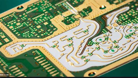
What is an RF PCB?
An RF PCB, or radio frequency printed circuit board, is a specialized type of PCB designed to work with high-frequency signals in wireless communication devices and systems. These circuit boards are engineered to minimize signal loss, distortion, and interference that can occur when dealing with radio frequencies, typically in the range of megahertz (MHz) to gigahertz (GHz).
RF PCBs are essential components in various applications, such as:
- Smartphones and tablets
- Wireless routers and access points
- Bluetooth devices
- GPS systems
- Radar and satellite communication equipment
Key Characteristics of RF PCBs
To effectively handle high-frequency signals, RF PCBs possess several distinct characteristics that set them apart from standard PCBs:
-
Material selection: RF PCBs are made using low-loss dielectric materials, such as Rogers RO4000 series, PTFE (Teflon), or ceramic-filled PTFE. These materials have a low dielectric constant and dissipation factor, which helps minimize signal loss and maintain signal integrity.
-
Controlled impedance: The traces on an RF PCB are designed to have a specific characteristic impedance (usually 50 ohms) to match the impedance of the connected components and minimize signal reflections. This is achieved through careful control of trace width, thickness, and spacing.
-
Shielding and grounding: To reduce electromagnetic interference (EMI) and crosstalk, RF PCBs often incorporate shielding techniques, such as ground planes, via fencing, and metal enclosures. Proper grounding is also crucial to provide a low-impedance return path for high-frequency currents.
-
Minimized trace length: Shorter traces help reduce signal loss and maintain signal integrity. RF PCB designers strive to keep trace lengths as short as possible and avoid unnecessary bends or turns that can cause reflections.
RF PCB Design Considerations
Designing an RF PCB requires a deep understanding of high-frequency circuit behavior and electromagnetic principles. Some key considerations include:
Transmission Line Theory
At radio frequencies, PCB traces behave like transmission lines rather than simple connections. Designers must consider factors such as characteristic impedance, propagation delay, and phase velocity when laying out traces.
Impedance Matching
To ensure maximum power transfer and minimize signal reflections, the impedance of the PCB traces must match the impedance of the connected components (e.g., antennas, amplifiers, and filters). Techniques such as stub matching and tapered lines are used to achieve impedance matching.
Electromagnetic Compatibility (EMC)
RF PCBs must be designed to minimize electromagnetic interference (EMI) and ensure electromagnetic compatibility (EMC) with other devices. This involves proper shielding, grounding, and filtering techniques, as well as adhering to regulatory standards such as FCC Part 15 and EN 55022.
Component Placement and Routing
The placement of components on an RF PCB is critical to minimize trace lengths, reduce crosstalk, and maintain signal integrity. Designers often use techniques such as microstrip and stripline routing to control impedance and minimize radiation.

RF PCB Manufacturing Process
Manufacturing an RF PCB requires specialized equipment and processes to ensure the highest quality and performance. The key steps in the manufacturing process include:
-
Material selection and preparation: The appropriate low-loss dielectric material is selected based on the application requirements. The material is then cut to size and cleaned to remove any contaminants.
-
Copper cladding: A layer of copper is laminated onto the dielectric material using heat and pressure. The copper thickness is chosen based on the desired trace thickness and current-carrying capacity.
-
Photolithography: The PCB layout is transferred onto the copper-clad board using a photoresist and UV exposure. The exposed areas are then chemically etched away, leaving the desired copper traces.
-
Via drilling: Holes are drilled through the board to create vias, which are used to connect traces on different layers.
-
Plating: The vias are plated with copper to ensure electrical continuity between layers. Additional plating, such as gold or silver, may be applied to improve conductivity and prevent oxidation.
-
Solder mask and silkscreen: A solder mask is applied to protect the copper traces from oxidation and prevent solder bridges. A silkscreen layer is added to provide component labels and other markings.
-
Surface finish: A surface finish, such as HASL (hot air solder leveling), ENIG (electroless nickel immersion gold), or OSP (organic solderability preservative), is applied to the exposed copper areas to improve solderability and protect against corrosion.
-
Electrical testing: The manufactured RF PCB undergoes rigorous electrical testing to ensure it meets the specified performance requirements, such as insertion loss, return loss, and crosstalk.

RF PCB Assembly Techniques
Assembling components onto an RF PCB requires specialized techniques to ensure proper performance and reliability. Some common assembly techniques include:
Surface Mount Technology (SMT)
SMT is the most widely used assembly technique for RF PCBs. Components are placed on the PCB surface and soldered using reflow or wave soldering processes. SMT allows for smaller component sizes and higher component density compared to through-hole mounting.
Chip-on-Board (COB)
COB is a technique where bare semiconductor die are directly attached to the PCB substrate using wire bonding or flip-chip bonding. This technique is often used for high-frequency and high-power applications, as it minimizes parasitic inductance and capacitance.
Hybrid Assembly
Hybrid assembly combines SMT and COB techniques to achieve the best performance and reliability. For example, an RF power amplifier may use SMT for passive components and COB for the active semiconductor die.

RF PCB Testing and Validation
To ensure the performance and reliability of an RF PCB, various testing and validation methods are employed:
Vector Network Analyzer (VNA) Testing
A VNA is used to measure the S-parameters of an RF PCB, which characterize its high-frequency performance. S-parameters include insertion loss, return loss, and crosstalk, among others.
Spectrum Analyzer Testing
A spectrum analyzer is used to measure the frequency response and power levels of an RF PCB. It can detect spurious emissions, harmonics, and other unwanted frequency components.
Electromagnetic Interference (EMI) Testing
EMI testing is performed to ensure that an RF PCB does not generate excessive electromagnetic interference that can disrupt other devices. This testing is often done in an anechoic chamber or a Faraday cage to minimize external interference.
Environmental Testing
RF PCBs are subjected to various environmental tests to ensure their reliability under different operating conditions. These tests may include:
- Temperature cycling
- Humidity exposure
- Vibration and shock testing
- Salt spray corrosion testing
Advantages of Using a Specialized RF PCB Assembly Service
Engaging a specialized RF PCB assembly service offers several advantages over in-house assembly or general PCB assembly services:
-
Expertise: RF PCB assembly requires specialized knowledge and experience in high-frequency circuit design and assembly techniques. A dedicated RF PCB assembly service has the necessary expertise to ensure optimal performance and reliability.
-
Specialized equipment: Assembling RF PCBs requires specialized equipment, such as high-precision pick-and-place machines, reflow soldering ovens, and wire bonding machines. A specialized assembly service has invested in this equipment and has the trained personnel to operate it effectively.
-
Quality control: A reputable RF PCB assembly service has rigorous quality control processes in place to ensure the highest level of workmanship and performance. This includes automated optical inspection (AOI), X-ray inspection, and functional testing.
-
Cost-effectiveness: Outsourcing RF PCB assembly to a specialized service can be more cost-effective than investing in in-house assembly capabilities, especially for low to medium volume production. The assembly service can leverage economies of scale and spread the cost of equipment and personnel across multiple customers.
-
Time-to-market: A specialized RF PCB assembly service can often provide faster turnaround times than in-house assembly, as they have streamlined processes and dedicated resources. This can help reduce time-to-market for new products.
Choosing the Right RF PCB Assembly Partner
When selecting an RF PCB assembly partner, consider the following factors:
-
Experience: Look for a company with a proven track record in RF PCB assembly, with experience in your specific application domain (e.g., wireless communications, radar, etc.).
-
Capabilities: Ensure that the company has the necessary equipment, processes, and expertise to handle your specific RF PCB assembly requirements, such as SMT, COB, or hybrid assembly.
-
Quality management: Choose a company with a robust quality management system, preferably certified to industry standards such as ISO 9001 or AS9100.
-
Communication and support: Good communication and responsive support are essential for a successful partnership. Look for a company that is proactive in providing updates and addressing any issues that may arise.
-
Pricing and lead times: While cost is an important factor, it should not be the sole deciding factor. Consider the value provided in terms of quality, reliability, and support. Also, ensure that the company can meet your required lead times and delivery schedules.
Conclusion
RF PCBs are critical components in today’s wireless communication devices and systems. Designing and manufacturing these high-frequency circuit boards requires specialized knowledge, equipment, and processes. Engaging a reputable RF PCB assembly service can provide significant advantages in terms of expertise, quality, and time-to-market.
When selecting an RF PCB assembly partner, consider factors such as experience, capabilities, quality management, communication, and pricing. By choosing the right partner, you can ensure the optimal performance and reliability of your RF PCBs, ultimately contributing to the success of your end products.
Frequently Asked Questions (FAQ)
1. What is the difference between an RF PCB and a standard PCB?
An RF PCB is specifically designed to handle high-frequency signals in the range of megahertz (MHz) to gigahertz (GHz). It is made using low-loss dielectric materials and has controlled impedance traces to minimize signal loss and maintain signal integrity. In contrast, a standard PCB is designed for lower frequency applications and may not have the same material properties or controlled impedance requirements.
2. What are the key design considerations for an RF PCB?
The key design considerations for an RF PCB include:
– Transmission line theory
– Impedance matching
– Electromagnetic compatibility (EMC)
– Component placement and routing
Designers must carefully consider these factors to ensure optimal high-frequency performance and minimize signal integrity issues.
3. What are the common assembly techniques for RF PCBs?
The common assembly techniques for RF PCBs include:
– Surface Mount Technology (SMT): Components are placed on the PCB surface and soldered using reflow or wave soldering processes.
– Chip-on-Board (COB): Bare semiconductor die are directly attached to the PCB substrate using wire bonding or flip-chip bonding.
– Hybrid Assembly: A combination of SMT and COB techniques to achieve the best performance and reliability.
4. What types of testing are performed on RF PCBs?
RF PCBs undergo various types of testing to ensure their performance and reliability, including:
– Vector Network Analyzer (VNA) Testing: Measures S-parameters to characterize high-frequency performance.
– Spectrum Analyzer Testing: Measures frequency response and power levels to detect spurious emissions and harmonics.
– Electromagnetic Interference (EMI) Testing: Ensures the PCB does not generate excessive EMI that can disrupt other devices.
– Environmental Testing: Subjects the PCB to temperature cycling, humidity exposure, vibration, and shock testing to ensure reliability under different operating conditions.
5. What are the advantages of using a specialized RF PCB assembly service?
The advantages of using a specialized RF PCB assembly service include:
– Expertise in high-frequency circuit design and assembly techniques
– Access to specialized equipment and trained personnel
– Rigorous quality control processes
– Cost-effectiveness compared to in-house assembly for low to medium volume production
– Faster time-to-market due to streamlined processes and dedicated resources
By engaging a reputable RF PCB assembly service, you can ensure the optimal performance and reliability of your RF PCBs while focusing on your core competencies.


Leave a Reply