Why is PCB Testing Important?
PCB testing is a critical step in the manufacturing process for several reasons:
- Quality Assurance: Testing helps identify defects and issues early in the manufacturing process, reducing the risk of faulty products reaching the end-user.
- Cost Savings: Early detection of problems can prevent the need for expensive rework or product recalls.
- Reliability: Thorough testing ensures that the PCB will function as intended, increasing the overall reliability of the electronic device.
- Compliance: Many industries have specific standards and regulations that PCBs must meet. Testing helps ensure compliance with these requirements.
13 Effective PCB Testing Methods
1. Visual Inspection
Visual inspection is the first step in PCB testing. It involves examining the board for any visible defects, such as:
- Incorrect component placement
- Solder bridging or insufficient solder
- Damaged or missing components
- Contamination or foreign objects
This process can be done manually by trained inspectors or using automated optical inspection (AOI) systems.
2. Automated Optical Inspection (AOI)
AOI systems use high-resolution cameras and image processing software to detect surface-level defects on the PCB. The system compares the captured images to a reference image of a known good board, identifying any discrepancies. AOI is particularly useful for detecting issues such as:
- Component misalignment
- Solder defects
- Incorrect component polarity
- Missing or damaged components
3. X-Ray Inspection
X-ray inspection is used to detect defects that are not visible on the surface of the PCB. This method is particularly useful for inspecting:
- Ball Grid Array (BGA) packages
- Flip-chip devices
- Voids in solder joints
- Internal component damage
X-ray systems use either 2D or 3D imaging techniques to create detailed images of the PCB’s internal structure.
4. In-Circuit Testing (ICT)
In-circuit testing involves using a bed-of-nails fixture to make electrical contact with specific points on the PCB. The tester then applies stimuli and measures the response at each point, comparing the results to expected values. ICT is effective for detecting:
- Short circuits
- Open circuits
- Incorrect component values
- Missing or incorrect components
5. Flying Probe Testing
Flying probe testing is an alternative to ICT that does not require a custom bed-of-nails fixture. Instead, it uses a set of movable probes that can be positioned anywhere on the PCB. The probes make electrical contact with test points, applying stimuli and measuring the response. Flying probe testing is more flexible than ICT but may be slower for high-volume production.
6. Boundary Scan Testing (JTAG)
Boundary scan testing, also known as JTAG (Joint Test Action Group) testing, is a method for testing the interconnections between digital components on a PCB. It uses a special test access port (TAP) built into the components to control and observe the behavior of the component’s input and output pins. Boundary scan testing is useful for detecting:
- Open or short circuits between components
- Stuck-at faults (pins stuck at a logical high or low)
- Incorrect component orientation
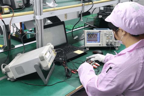
7. Functional Testing
Functional testing involves powering up the PCB and testing its operation under normal conditions. This method verifies that the board performs as intended, with all components and subsystems working together correctly. Functional testing may include:
- Power-on self-test (POST)
- Firmware or software testing
- Real-world scenario testing
- Stress testing under various environmental conditions
8. Burn-In Testing
Burn-in testing is a method of accelerating the aging process of a PCB to identify early-life failures. The board is subjected to elevated temperatures and voltages for an extended period, typically 24 to 48 hours. This process helps identify components prone to infant mortality, ensuring that only reliable boards are shipped to customers.
9. Thermal Imaging
Thermal imaging is used to detect hotspots and thermal issues on a PCB. An infrared camera captures the temperature distribution across the board, highlighting areas that are generating excessive heat. This information can help identify:
- Overloaded components
- Insufficient cooling
- Power supply issues
- Design flaws that lead to thermal problems
10. Electromagnetic Compatibility (EMC) Testing
EMC testing ensures that the PCB does not generate excessive electromagnetic interference (EMI) and can operate reliably in the presence of external EMI. This testing is crucial for compliance with regulatory standards and to prevent interference with other electronic devices. EMC testing may include:
- Radiated emissions testing
- Conducted emissions testing
- Electromagnetic susceptibility testing
11. Residual Current Testing (Hipot)
Residual current testing, also known as hipot (high potential) testing, is used to verify the electrical insulation between different parts of the PCB. A high voltage is applied between various points on the board, and the leakage current is measured. This test helps identify:
- Insulation breakdowns
- Clearance and creepage distance issues
- Potential safety hazards
12. Acoustic Microscopy
Acoustic microscopy is a non-destructive testing method that uses high-frequency sound waves to create images of the internal structure of a PCB. This technique is particularly useful for detecting:
- Delamination
- Voids in solder joints
- Cracks in components or substrates
- Disbonds between layers
Acoustic microscopy can provide detailed images without the need for physical sectioning of the board.
13. Environmental Testing
Environmental testing exposes the PCB to various environmental conditions to ensure its reliability and durability. These tests may include:
- Temperature cycling
- Humidity testing
- Vibration and shock testing
- Altitude testing
- Salt spray testing
Environmental testing helps identify potential weaknesses in the design or manufacturing process that could lead to premature failure in the field.

PCB Testing Comparison
| Test Method | Detects | Speed | Cost |
|---|---|---|---|
| Visual Inspection | Surface defects | Slow | Low |
| AOI | Surface defects | Fast | Moderate |
| X-Ray Inspection | Internal defects | Moderate | High |
| ICT | Component and connectivity issues | Fast | High |
| Flying Probe Testing | Component and connectivity issues | Moderate | Moderate |
| Boundary Scan Testing | Interconnect and component issues | Fast | Low |
| Functional Testing | Operational issues | Moderate | Moderate |
| Burn-In Testing | Early-life failures | Slow | Moderate |
| Thermal Imaging | Thermal issues | Fast | Moderate |
| EMC Testing | Electromagnetic compatibility | Moderate | High |
| Residual Current Testing | Insulation issues | Fast | Moderate |
| Acoustic Microscopy | Internal defects | Slow | High |
| Environmental Testing | Reliability and durability | Slow | High |

Frequently Asked Questions (FAQ)
-
Q: What is the most important PCB testing method?
A: There is no single most important PCB testing method. Each method addresses different aspects of the board’s quality and reliability. A comprehensive testing strategy should include a combination of methods based on the specific requirements of the product and industry. -
Q: Can all PCB testing methods be automated?
A: Many PCB testing methods can be automated, such as AOI, X-ray inspection, ICT, and flying probe testing. However, some methods, like visual inspection and functional testing, may require human intervention or judgment. -
Q: How often should PCB testing be performed?
A: PCB testing should be performed at various stages of the manufacturing process, including prototype development, pre-production, and volume production. The frequency of testing depends on factors such as product complexity, production volume, and quality requirements. -
Q: What are the consequences of inadequate PCB testing?
A: Inadequate PCB testing can lead to several negative consequences, including: - Increased defect rates and product returns
- Higher production costs due to rework and scrap
- Delays in time-to-market
- Damage to brand reputation
-
Potential safety hazards for end-users
-
Q: How do I choose the right PCB testing methods for my product?
A: When selecting PCB testing methods, consider the following factors: - Product complexity and design
- Industry-specific standards and regulations
- Production volume and throughput requirements
- Available budget and resources
- Potential failure modes and their impact on product performance
Consult with experienced PCB manufacturing and testing partners to develop a comprehensive testing strategy tailored to your product’s needs.

Conclusion
Effective PCB testing is essential for ensuring the quality, reliability, and safety of electronic devices. By implementing a combination of the 13 test methods discussed in this article, manufacturers can identify and address a wide range of potential issues, from surface-level defects to internal component failures. A well-designed testing strategy not only helps prevent costly rework and product recalls but also enhances customer satisfaction and brand reputation.
As PCB technology continues to evolve, with increasing complexity and miniaturization, the importance of thorough testing will only grow. Manufacturers must stay up-to-date with the latest testing methods and technologies to remain competitive and meet the ever-changing demands of the electronics industry.


Leave a Reply