Introduction to PCB Assembly
PCB assembly is the process of assembling electronic components onto a printed circuit board (PCB) to create a functional electronic device. The PCB serves as the foundation for the electronic components, providing electrical connections and mechanical support. PCB assembly involves various techniques and processes, including surface mount technology (SMT) and through-hole technology (THT), to ensure the proper placement and soldering of components onto the PCB.
The Importance of PCB Assembly
PCB assembly plays a crucial role in the electronics industry, as it enables the production of complex electronic devices in a compact and efficient manner. Some of the key benefits of PCB assembly include:
-
Miniaturization: PCB assembly allows for the creation of smaller and more compact electronic devices, which is essential in today’s world of portable and wearable electronics.
-
Reliability: Properly assembled PCBs ensure reliable electrical connections and minimize the risk of component failure, resulting in more dependable electronic devices.
-
Cost-effectiveness: PCB assembly streamlines the manufacturing process, reducing labor costs and increasing production efficiency, making it a cost-effective solution for electronic device production.
-
Flexibility: PCB assembly can accommodate a wide range of electronic components and design requirements, allowing for the creation of custom electronic devices tailored to specific applications.
PCB Assembly Process
The PCB assembly process involves several steps, each of which is critical to ensuring the quality and functionality of the final product. The main stages of PCB assembly include:
1. PCB Design and Fabrication
Before the assembly process can begin, the PCB must be designed and fabricated. This involves creating a schematic diagram of the electronic circuit, converting it into a PCB layout, and then manufacturing the physical PCB. The PCB design process takes into account factors such as component placement, signal integrity, and thermal management to ensure optimal performance of the final product.
2. Solder Paste Application
Once the PCB is fabricated, the first step in the assembly process is the application of solder paste onto the PCB pads. Solder paste is a mixture of tiny solder particles suspended in a flux medium. The most common method for applying solder paste is through the use of a stencil, which is a thin metal sheet with apertures that correspond to the PCB pads. The stencil is placed over the PCB, and solder paste is spread across the stencil using a squeegee, depositing the paste onto the pads.
3. Component Placement
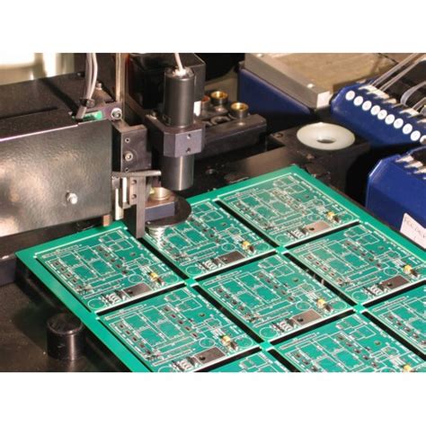
After the solder paste is applied, the electronic components are placed onto the PCB. For SMT components, this is typically done using a pick-and-place machine, which uses vacuum nozzles to pick up components from tape reels or trays and place them onto the PCB with high precision. THT components are usually inserted manually or with the help of insertion machines.
4. Reflow Soldering
Once all the components are placed, the PCB undergoes reflow soldering. In this process, the PCB is passed through a reflow oven, which applies a carefully controlled temperature profile to melt the solder paste and form a permanent electrical and mechanical bond between the components and the PCB pads. The temperature profile is critical to ensure proper solder joint formation and to prevent damage to the components or the PCB.
5. Inspection and Testing
After reflow soldering, the assembled PCB undergoes visual inspection and electrical testing to ensure that all components are properly soldered and that the board functions as intended. Visual inspection may be done manually or using automated optical inspection (AOI) systems, which use cameras and image processing algorithms to detect soldering defects or missing components. Electrical testing may involve in-circuit testing (ICT), flying probe testing, or functional testing, depending on the complexity and requirements of the PCB.
6. Cleaning and Coating
If required, the assembled PCB may undergo cleaning to remove any flux residue or contaminants from the soldering process. This is typically done using ultrasonic cleaning or inline washing systems. After cleaning, the PCB may also receive a protective coating, such as conformal coating, to enhance its durability and resistance to environmental factors like moisture, dust, or chemicals.
7. Final Assembly and Packaging
Finally, the assembled and tested PCB is integrated into the final product, which may involve additional steps such as mounting in an enclosure, connecting to other sub-assemblies, or programming firmware. The finished product is then packaged and ready for distribution.

Surface Mount Technology (SMT) vs. Through-Hole Technology (THT)
PCB assembly can be broadly categorized into two main technologies: surface mount technology (SMT) and through-hole technology (THT). Each technology has its own advantages and disadvantages, and the choice between them depends on factors such as the type of components, the required level of miniaturization, and the production volume.
Surface Mount Technology (SMT)
SMT is a modern PCB assembly technology that involves placing components directly onto the surface of the PCB. SMT components have small metal leads or terminations that are soldered to pads on the PCB surface. Some of the key advantages of SMT include:
-
Miniaturization: SMT components are generally smaller than THT components, allowing for higher component density and more compact PCB designs.
-
Faster assembly: SMT assembly is highly automated, using pick-and-place machines and reflow soldering, which enables faster production times and higher throughput.
-
Lower cost: SMT assembly requires less manual labor and fewer drilling operations compared to THT, resulting in lower production costs, especially for high-volume production.
-
Better performance: SMT components have shorter lead lengths, which reduces parasitic effects and improves signal integrity, resulting in better high-frequency performance.
However, SMT also has some limitations:
-
Limited power handling: SMT components generally have lower power handling capabilities compared to THT components due to their smaller size and limited heat dissipation.
-
Rework challenges: Reworking or replacing SMT components can be more difficult and time-consuming compared to THT components, as the components are soldered directly to the PCB surface.
Through-Hole Technology (THT)
THT is a traditional PCB assembly technology that involves inserting component leads through holes drilled in the PCB and soldering them to pads on the opposite side of the board. Some of the key advantages of THT include:
-
Mechanical strength: THT components are mechanically secured to the PCB by their leads, providing greater mechanical strength and durability compared to SMT components.
-
Power handling: THT components can handle higher power levels due to their larger size and better heat dissipation through the PCB.
-
Ease of rework: THT components are easier to rework or replace, as they can be desoldered and removed from the PCB without damaging the board or nearby components.
However, THT also has some limitations:
-
Larger size: THT components are generally larger than SMT components, requiring more PCB space and limiting the level of miniaturization.
-
Slower assembly: THT assembly is more labor-intensive and requires manual insertion of components, resulting in slower production times and lower throughput compared to SMT.
-
Higher cost: THT assembly is generally more expensive than SMT assembly due to the higher labor costs and the need for drilling operations.
In modern PCB assembly, it is common to use a combination of SMT and THT technologies, depending on the specific requirements of the electronic device. This hybrid approach allows designers to take advantage of the benefits of both technologies while minimizing their limitations.

PCB Assembly Services
Given the complexity and precision required for PCB assembly, many companies choose to outsource this process to specialized PCB assembly service providers. These providers offer a range of services, from PCB design and fabrication to component sourcing, assembly, and testing. Some of the key advantages of using PCB assembly services include:
-
Expertise: PCB assembly service providers have the knowledge, skills, and experience to handle a wide range of PCB assembly projects, ensuring high-quality results and adherence to industry standards.
-
Advanced equipment: PCB assembly service providers invest in state-of-the-art equipment and technology, such as high-precision pick-and-place machines, reflow ovens, and automated inspection systems, which may not be economically feasible for individual companies to acquire and maintain.
-
Scalability: PCB assembly service providers can accommodate projects of various scales, from small prototype runs to large-volume production, allowing companies to scale their production up or down as needed.
-
Cost-effectiveness: Outsourcing PCB assembly can be more cost-effective than setting up and maintaining an in-house assembly line, especially for companies with limited production volumes or those that require specialized assembly capabilities.
When choosing a PCB assembly service provider, it is important to consider factors such as their experience, capabilities, quality control processes, turnaround times, and customer support. Additionally, it is crucial to provide the service provider with accurate and complete documentation, including PCB designs, bill of materials (BOM), and assembly instructions, to ensure a smooth and successful assembly process.

Quality Control in PCB Assembly
Ensuring the quality of assembled PCBs is critical to the reliability and performance of the final electronic device. PCB assembly service providers employ various quality control measures throughout the assembly process to identify and prevent defects. Some of the common quality control techniques used in PCB assembly include:
-
Automated Optical Inspection (AOI): AOI systems use cameras and image processing algorithms to inspect assembled PCBs for defects such as missing components, incorrect component placement, or soldering issues. AOI can quickly and accurately identify defects, reducing the need for manual inspection and improving overall quality.
-
X-Ray Inspection: X-ray inspection is used to examine solder joints and other hidden features that are not visible to the naked eye or AOI systems. This technique is particularly useful for inspecting ball grid array (BGA) and other high-density components.
-
In-Circuit Testing (ICT): ICT involves using a bed-of-nails fixture to make electrical contact with specific points on the PCB and verify the presence, orientation, and value of components, as well as the integrity of the electrical connections. ICT can identify defects such as short circuits, open circuits, or incorrect component values.
-
Flying Probe Testing: Flying probe testing uses movable test probes to make electrical contact with specific points on the PCB, similar to ICT. However, flying probe testing does not require a custom fixture, making it more flexible and adaptable to different PCB designs.
-
Functional Testing: Functional testing involves powering up the assembled PCB and verifying its performance against a set of predefined test cases. This testing ensures that the PCB functions as intended and meets the specified requirements.
By implementing a combination of these quality control techniques, PCB assembly service providers can identify and address defects early in the assembly process, reducing the risk of faulty products reaching the end-user and minimizing the cost and time associated with rework and repairs.
Design for Manufacturing (DFM) Considerations
To ensure the success of a PCB assembly project, it is important to consider Design for Manufacturing (DFM) principles during the PCB design phase. DFM involves designing the PCB in a way that optimizes its manufacturability, reliability, and cost-effectiveness. Some key DFM considerations for PCB assembly include:
-
Component selection: Choose components that are readily available, have standard packaging, and are compatible with the selected assembly technology (SMT or THT). Avoid using obsolete or hard-to-source components, as this can lead to supply chain issues and delays.
-
Footprint and pad design: Ensure that component footprints and pad sizes are appropriate for the selected components and assembly technology. Follow the manufacturer’s recommendations and industry standards for pad dimensions, spacing, and orientation.
-
Placement and routing: Place components in a way that facilitates assembly and minimizes the risk of defects. Ensure adequate spacing between components for pick-and-place machines and soldering processes. Route traces in a way that minimizes cross-talk, signal integrity issues, and electromagnetic interference (EMI).
-
Solder mask and silkscreen: Use solder mask to protect the PCB from oxidation and prevent solder bridges between closely spaced pads. Apply silkscreen markings to identify components, polarity, and other important information, making the PCB easier to assemble and debug.
-
Panelization: If producing multiple PCBs, consider panelizing the design to optimize material usage and assembly efficiency. Incorporate appropriate panelization features, such as breakaway tabs or mousebites, to facilitate depanelization without damaging the individual boards.
By incorporating DFM principles into the PCB design process, designers can streamline the assembly process, reduce the risk of defects, and ultimately lower the overall cost of production.
Future Trends in PCB Assembly
As the electronics industry continues to evolve, PCB assembly technologies and processes are also advancing to keep pace with new challenges and opportunities. Some of the key trends shaping the future of PCB assembly include:
-
Miniaturization: The demand for smaller, more compact electronic devices is driving the adoption of advanced packaging technologies, such as chip-scale packaging (CSP) and wafer-level packaging (WLP), which enable the integration of even smaller components onto PCBs.
-
High-density interconnect (HDI): HDI PCBs feature finer traces, smaller vias, and higher layer counts, allowing for greater component density and improved signal integrity. As electronic devices become more complex and compact, the use of HDI technology in PCB assembly is expected to grow.
-
Flexible and Rigid-Flex PCBs: Flexible and rigid-flex PCBs are gaining popularity in applications that require conformity to irregular shapes or improved mechanical durability. These PCBs can be folded, bent, or twisted, making them ideal for wearable electronics, medical devices, and aerospace applications.
-
3D printing: Additive manufacturing techniques, such as 3D printing, are being explored for PCB fabrication and assembly. 3D printing allows for the creation of complex, non-planar PCB structures and the embedding of components within the PCB itself, opening up new possibilities for electronic device design and integration.
-
Automation and Industry 4.0: PCB assembly is increasingly embracing automation and digitalization, in line with the principles of Industry 4.0. Advanced technologies, such as robotic process automation (RPA), machine learning, and the Internet of Things (IoT), are being applied to optimize assembly processes, improve quality control, and enable real-time monitoring and data-driven decision making.
As these trends continue to shape the PCB assembly landscape, electronics manufacturers and PCB assembly service providers will need to adapt and innovate to stay competitive and meet the evolving needs of their customers.
FAQs
-
What is the difference between PCB assembly and PCB fabrication?
PCB fabrication refers to the process of manufacturing the bare printed circuit board, which includes designing the PCB layout, printing the circuit patterns, and laminating the layers. PCB assembly, on the other hand, involves populating the fabricated PCB with electronic components and soldering them in place to create a functional electronic assembly. -
What are the most common PCB assembly defects, and how can they be prevented?
Some of the most common PCB assembly defects include solder bridges, cold solder joints, tombstoning (when a component stands up on one end), and component misalignment. These defects can be prevented by ensuring proper solder paste application, optimizing reflow soldering profiles, and implementing robust quality control processes, such as automated optical inspection (AOI) and X-ray inspection. -
What is the difference between lead-based and lead-free soldering in PCB assembly?
Lead-based soldering uses a tin-lead alloy, typically with a composition of 63% tin and 37% lead (Sn63/Pb37). Lead-free soldering, which has become more prevalent due to environmental and health concerns, uses alloys that do not contain lead, such as tin-silver-copper (SAC) alloys. Lead-free soldering requires higher reflow temperatures and may be more susceptible to certain defects, such as tin whiskers. -
How do I choose the right PCB assembly service provider for my project?
When selecting a PCB assembly service provider, consider factors such as their experience, technical capabilities, quality control processes, and customer support. Look for providers that have a proven track record in assembling PCBs similar to your project, and that can meet your specific requirements for turnaround time, volume, and cost. It is also important to ensure that the provider can handle your specific components and assembly technologies (e.g., SMT, THT, or mixed). -
What information do I need to provide to a PCB assembly service provider to get started?
To begin a PCB assembly project, you will typically need to provide the PCB assembly service provider with the following information: - PCB design files (e.g., Gerber files, ODB++, or IPC-2581)
- Bill of Materials (BOM), which lists all the components required for the assembly
- Assembly drawings or instructions, indicating component placement and orientation
- Any special requirements or constraints, such as specific soldering profiles, testing requirements, or packaging instructions
By providing accurate and complete information upfront, you can help ensure a smooth and successful PCB assembly process.
Conclusion
PCB assembly is a critical process in the production of electronic devices, involving the integration of electronic components onto a printed circuit board to create a functional assembly. The process encompasses various technologies and techniques, including surface mount technology (SMT) and through-hole technology (THT), each with its own advantages and limitations.
To ensure the success of a PCB assembly project, it is important to consider factors such as design for manufacturing (DFM), component selection, and quality control processes. Partnering with an experienced and capable


Leave a Reply