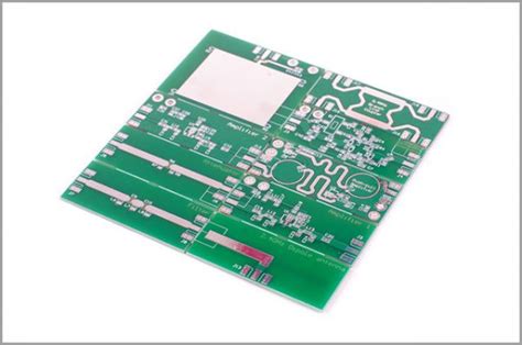
What is Panelization PCB?
Panelization PCB, also known as PCB Panel or PCB Array, is a process of combining multiple identical or different printed circuit board designs onto a single panel for manufacturing. This technique is widely used in the electronics industry to increase production efficiency, reduce costs, and optimize material usage.
Benefits of Panelization PCB
- Cost reduction: Panelizing PCBs allows for the production of multiple boards in a single run, reducing setup time and costs.
- Increased efficiency: Manufacturing panels instead of individual boards streamlines the assembly process and reduces handling time.
- Improved quality: Panelization ensures consistent quality across all boards in the panel, as they are produced under the same conditions.
- Optimized material usage: Arranging boards on a panel minimizes waste material, leading to more environmentally friendly production.
PCB Panelization Techniques
There are several techniques used for PCB panelization, each with its own advantages and disadvantages. The choice of technique depends on factors such as the board design, manufacturing requirements, and end-use application.
Tab Routing
Tab routing is a popular panelization method that involves connecting individual boards with small tabs. These tabs are milled or routed out after the assembly process, allowing for easy separation of the boards.
Advantages:
– Simple and cost-effective
– Suitable for low-volume production
– Allows for easy board separation
Disadvantages:
– Tabs can leave rough edges on the boards
– Not suitable for high-density designs or boards with tight tolerances
V-Scoring
V-scoring involves creating V-shaped grooves between the individual boards on the panel. These grooves allow for easy snapping of the boards after assembly.
Advantages:
– Provides clean and smooth board edges
– Suitable for high-volume production
– Allows for easy board separation
Disadvantages:
– Requires specialized equipment for creating V-grooves
– May not be suitable for thick or rigid PCBs
Perforated Tabs
Perforated tabs are similar to tab routing, but instead of solid tabs, they feature a series of small holes or perforations. These perforations allow for easy separation of the boards by breaking along the perforated lines.
Advantages:
– Provides cleaner board edges compared to tab routing
– Suitable for medium to high-volume production
– Allows for easy board separation
Disadvantages:
– May require additional processing time for creating perforations
– Not suitable for boards with delicate components near the perforations

PCB Panelization Design Considerations
When designing a PCB panel, several factors must be considered to ensure optimal manufacturing results and end-product quality.
Board Spacing and Clearance
Proper spacing between individual boards on the panel is crucial for maintaining the structural integrity of the panel and ensuring clean separation of the boards. The minimum spacing between boards depends on the panelization technique used and the manufacturer’s specifications.
| Panelization Technique | Minimum Board Spacing |
|---|---|
| Tab Routing | 2 mm |
| V-Scoring | 1.5 mm |
| Perforated Tabs | 2.5 mm |
Fiducial Marks and Tooling Holes
Fiducial marks and tooling holes are essential for accurate alignment and registration during the manufacturing process. Fiducial marks are small, round, or cross-shaped markers placed on the panel that serve as reference points for automated assembly equipment. Tooling holes are used to secure the panel during various manufacturing steps.
When placing fiducial marks and tooling holes, consider the following:
- Place fiducial marks near the corners of the panel and individual boards
- Ensure fiducial marks are visible and unobstructed
- Use a minimum of three tooling holes per panel
- Follow the manufacturer’s specifications for tooling hole size and placement
Panelization Border and Waste Material
The panelization border is the area around the perimeter of the panel that is used for handling, tooling, and other manufacturing purposes. It is essential to include an adequate border to ensure the panel’s stability and to provide space for necessary markings and information.
When designing the panelization border, consider the following:
- Include a minimum border of 5 mm around the panel
- Incorporate panel identification markings, such as part numbers and revision codes
- Minimize waste material by optimizing board placement and orientation

PCB Panelization Manufacturing Process
The PCB panelization manufacturing process involves several steps, from panel design to final assembly and testing.
Panel Design and Preparation
- Create individual board designs using PCB design software
- Arrange boards on the panel, considering spacing, clearance, and orientation
- Add fiducial marks, tooling holes, and identification markings
- Generate manufacturing files (Gerber, drill, and assembly files)
PCB Fabrication
- Manufacture the bare PCB panel using standard PCB fabrication processes (etching, drilling, plating, etc.)
- Apply solder mask and silkscreen to the panel
- Perform electrical testing on the bare panel to ensure functionality
Component Assembly
- Apply solder paste to the panel using a stencil or screen printing process
- Place components on the panel using automated pick-and-place equipment
- Reflow the panel to permanently attach the components
- Perform visual inspection and automated optical inspection (AOI) to verify component placement and soldering quality
Panel Depanelization
- Separate individual boards from the panel using the chosen panelization technique (tab routing, V-scoring, or perforated tabs)
- Clean and inspect the individual boards for any damage or defects
- Perform final electrical testing on the individual boards to ensure functionality
Packaging and Shipping
- Package the individual boards according to customer or industry specifications
- Label and ship the boards to the end customer or next stage of the manufacturing process

Frequently Asked Questions (FAQ)
1. What is the minimum board thickness for PCB panelization?
The minimum board thickness for PCB panelization depends on the chosen panelization technique and the manufacturer’s capabilities. Generally, a minimum thickness of 0.8 mm is recommended for tab routing and perforated tabs, while V-scoring can accommodate thinner boards down to 0.6 mm.
2. Can different board designs be combined on the same panel?
Yes, different board designs can be combined on the same panel, known as a mixed panel or multi-array panel. This approach is useful for low-volume production runs or when different board designs share similar specifications and materials.
3. How does PCB panelization affect the cost of production?
PCB panelization can significantly reduce the cost of production by minimizing setup time, material waste, and handling. By producing multiple boards on a single panel, manufacturers can optimize their processes and resources, resulting in lower per-unit costs for the end customer.
4. What are the most common panel sizes used in PCB manufacturing?
Common panel sizes used in PCB manufacturing include:
- 18″ x 24″ (457 mm x 610 mm)
- 21″ x 24″ (533 mm x 610 mm)
- 18″ x 21″ (457 mm x 533 mm)
- 16″ x 18″ (406 mm x 457 mm)
The choice of panel size depends on the manufacturer’s equipment capabilities, the individual board dimensions, and the panelization technique used.
5. Can PCB panelization be used for flexible circuits?
Yes, PCB panelization can be used for flexible circuits, although the process may require specialized techniques and materials. Flexible circuit panelization often involves the use of carrier panels or special adhesives to maintain the stability of the flexible material during manufacturing.
Conclusion
PCB panelization is a critical process in the electronics manufacturing industry, offering numerous benefits such as cost reduction, increased efficiency, and improved quality. By understanding the various panelization techniques, design considerations, and manufacturing processes, engineers and manufacturers can optimize their PCB production and deliver high-quality products to their customers.
As the electronics industry continues to evolve, with increasingly complex designs and smaller form factors, PCB panelization will remain an essential tool for meeting the demands of modern electronics manufacturing.


Leave a Reply