What is PCB Panelization?
PCB panelization is the process of grouping multiple identical or different PCB designs onto a single panel for fabrication and assembly. The main goal of panelization is to maximize the utilization of the manufacturing resources, minimize material waste, and reduce the overall production time and costs.
Benefits of PCB Panelization
- Increased production efficiency
- Reduced manufacturing costs
- Improved material utilization
- Faster assembly process
- Consistent quality across multiple boards
Types of PCB Panelization Methods
There are several PCB panelization methods available, each with its own advantages and disadvantages. The choice of the panelization method depends on factors such as the PCB design, manufacturing requirements, and the intended application. Let’s explore the most common PCB panelization methods in detail.
1. Tab Routing Panelization
Tab routing panelization is one of the most popular and cost-effective methods for PCB panelization. In this method, individual PCBs are connected to the panel frame using small tabs, which are later removed after the assembly process. The tabs provide mechanical support to the boards during fabrication and assembly.
Advantages of Tab Routing Panelization
- Cost-effective method
- Suitable for high-volume production
- Allows for easy separation of individual boards
- Provides good mechanical support during fabrication and assembly
Disadvantages of Tab Routing Panelization
- Requires additional space for the tabs
- May leave rough edges on the boards after tab removal
- Limited design flexibility due to the need for uniform tab placement
2. V-Scoring Panelization
V-scoring panelization involves creating V-shaped grooves along the perimeter of individual PCBs on the panel. These grooves allow for easy separation of the boards after the assembly process. V-scoring is often used for smaller PCBs or when a clean edge finish is required.
Advantages of V-Scoring Panelization
- Provides clean edge finish after separation
- Suitable for smaller PCBs
- Allows for closer placement of boards on the panel
- Reduces the risk of damage during separation
Disadvantages of V-Scoring Panelization
- Higher cost compared to tab routing
- Requires specialized equipment for creating the V-grooves
- May weaken the board structure if the grooves are too deep
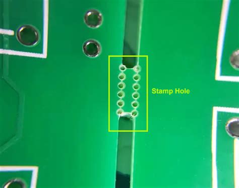
3. Perforated Panelization
Perforated panelization involves creating a series of small holes along the perimeter of individual PCBs on the panel. These perforations allow for easy separation of the boards after the assembly process. This method is often used for medium to large-sized PCBs or when a clean edge finish is not critical.
Advantages of Perforated Panelization
- Cost-effective method
- Suitable for medium to large-sized PCBs
- Allows for easy separation of individual boards
- Provides good mechanical support during fabrication and assembly
Disadvantages of Perforated Panelization
- May leave rough edges on the boards after separation
- Requires additional space for the perforations
- Limited design flexibility due to the need for uniform perforation placement
4. Snap-Apart Panelization
Snap-apart panelization is a method where individual PCBs are connected to the panel frame using small, breakable tabs called Mouse Bites. These mouse bites allow for easy separation of the boards by simply snapping them apart after the assembly process. This method is often used for prototyping or low-volume production.
Advantages of Snap-Apart Panelization
- Cost-effective method for low-volume production or prototyping
- Allows for easy separation of individual boards
- Provides good mechanical support during fabrication and assembly
- Suitable for a wide range of board sizes
Disadvantages of Snap-Apart Panelization
- May leave rough edges on the boards after separation
- Requires additional space for the mouse bites
- Limited design flexibility due to the need for uniform mouse bite placement
- Not suitable for high-volume production
5. Laser Panelization
Laser panelization is a high-precision method that uses a laser to create perforations or cut lines along the perimeter of individual PCBs on the panel. This method allows for highly accurate and clean separation of the boards after the assembly process. Laser panelization is often used for high-density or complex PCB designs.
Advantages of Laser Panelization
- Provides high-precision and clean edge finish after separation
- Suitable for high-density or complex PCB designs
- Allows for closer placement of boards on the panel
- Reduces the risk of damage during separation
Disadvantages of Laser Panelization
- Higher cost compared to other panelization methods
- Requires specialized laser equipment
- May have limitations on the thickness of the PCB material

Factors to Consider When Choosing a PCB Panelization Method
When selecting a PCB panelization method, several factors should be considered to ensure the best results for your specific project. These factors include:
- PCB design complexity
- Manufacturing requirements
- Production volume
- Material properties
- Cost considerations
- Edge finish requirements
- Assembly process compatibility
By carefully evaluating these factors, you can choose the most suitable panelization method that meets your project’s needs and budget.

Best Practices for PCB Panelization
To ensure successful PCB panelization, follow these best practices:
- Consult with your PCB manufacturer early in the design process to discuss panelization options and requirements.
- Provide clear and detailed panelization instructions to your manufacturer, including the desired method, panel dimensions, and any specific requirements.
- Consider the spacing between individual boards on the panel to allow for proper tooling and assembly processes.
- Incorporate fiducial marks and tooling holes in your panel design to aid in alignment and registration during fabrication and assembly.
- Verify the compatibility of your chosen panelization method with the intended assembly process, such as pick-and-place machines or reflow soldering.
- Conduct thorough testing and validation of your panelized PCB design before proceeding with full-scale production.

PCB Panelization Methods Comparison
| Panelization Method | Advantages | Disadvantages |
|---|---|---|
| Tab Routing | – Cost-effective – Suitable for high-volume production – Easy separation of boards – Good mechanical support |
– Requires additional space for tabs – May leave rough edges after tab removal – Limited design flexibility |
| V-Scoring | – Clean edge finish after separation – Suitable for smaller PCBs – Closer placement of boards – Reduces risk of damage during separation |
– Higher cost compared to tab routing – Requires specialized equipment – May weaken board structure if grooves are too deep |
| Perforated | – Cost-effective – Suitable for medium to large-sized PCBs – Easy separation of boards – Good mechanical support |
– May leave rough edges after separation – Requires additional space for perforations – Limited design flexibility |
| Snap-Apart | – Cost-effective for low-volume or prototyping – Easy separation of boards – Good mechanical support – Suitable for various board sizes |
– May leave rough edges after separation – Requires additional space for mouse bites – Limited design flexibility – Not suitable for high-volume production |
| Laser | – High-precision and clean edge finish – Suitable for high-density or complex designs – Closer placement of boards – Reduces risk of damage during separation |
– Higher cost compared to other methods – Requires specialized laser equipment – May have limitations on PCB material thickness |
Frequently Asked Questions (FAQ)
-
Q: What is the most cost-effective PCB panelization method for high-volume production?
A: Tab routing panelization is generally the most cost-effective method for high-volume production, as it provides good mechanical support and allows for easy separation of individual boards. -
Q: Which panelization method is best suited for achieving a clean edge finish on the separated PCBs?
A: V-scoring and laser panelization methods provide the cleanest edge finish after separating the individual PCBs from the panel. -
Q: Can different panelization methods be combined on a single panel?
A: Yes, different panelization methods can be combined on a single panel, depending on the specific requirements of the PCB design and the manufacturing process. However, this may increase the complexity and cost of the panelization process. -
Q: How does PCB panelization affect the overall manufacturing cost?
A: PCB panelization can significantly reduce the overall manufacturing cost by optimizing material usage, increasing production efficiency, and minimizing handling time. However, the choice of panelization method and the specific design requirements can impact the cost savings. -
Q: What should I consider when choosing a panelization method for my PCB project?
A: When choosing a panelization method, consider factors such as the PCB design complexity, manufacturing requirements, production volume, material properties, cost considerations, edge finish requirements, and assembly process compatibility. Consult with your PCB manufacturer to determine the best panelization method for your specific project.
Conclusion
PCB panelization is a crucial process in the manufacturing of printed circuit boards, offering numerous benefits such as increased production efficiency, reduced costs, and improved material utilization. By understanding the various panelization methods available and their advantages and disadvantages, you can make an informed decision when selecting the most suitable method for your PCB project.
When choosing a PCB panelization method, consider factors such as the design complexity, manufacturing requirements, production volume, and cost considerations. Consult with your PCB manufacturer early in the design process to ensure the best results and follow best practices for successful panelization.
By implementing the appropriate PCB panelization method and following best practices, you can optimize your PCB manufacturing process, reduce costs, and improve the overall quality of your printed circuit boards.


Leave a Reply