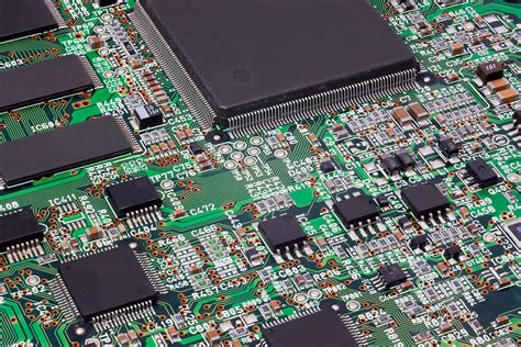
Introduction to PCB Assembly
PCB assembly is the process of attaching electronic components to a printed circuit board (PCB) to create a functional electronic device. It involves soldering components onto the PCB, which is a complex process that requires precision and accuracy. PCB assembly is a crucial step in the manufacturing of electronic devices, as it determines the reliability and performance of the final product.
Types of PCB Assembly
There are two main types of PCB assembly: through-hole and surface-mount.
- Through-hole assembly involves inserting component leads through holes drilled in the PCB and soldering them to pads on the opposite side.
- Surface-mount assembly involves placing components directly onto pads on the surface of the PCB and soldering them in place.
Surface-mount assembly has become increasingly popular in recent years due to its ability to accommodate smaller components and higher component densities.
The Importance of Choosing the Right EMS Provider for Complex PCB Assembly
When it comes to assembling complex PCBs, choosing the right electronic manufacturing services (EMS) provider is crucial. Complex PCBs often have high component densities, fine pitch sizes, and strict tolerance requirements, which require specialized equipment and expertise to assemble properly.
Factors to Consider When Choosing an EMS Provider
- Experience and Expertise: Look for an EMS provider with a proven track record of assembling complex PCBs. They should have experience working with a wide range of components and PCB designs.
- Quality Control: Quality is critical when it comes to complex PCB assembly. Choose an EMS provider with strict quality control measures in place, including automated optical inspection (AOI) and X-ray inspection.
- Technology and Equipment: Complex PCB assembly requires advanced technology and equipment, such as high-speed pick-and-place machines and reflow ovens. Make sure your EMS provider has the necessary equipment to handle your specific PCB design.
- Communication and Collaboration: Clear communication and collaboration between you and your EMS provider are essential for successful complex PCB assembly. Look for a provider that is responsive and willing to work closely with you throughout the manufacturing process.

The Benefits of One-Stop PCB Assembly
One-stop PCB assembly refers to an EMS provider that offers a complete range of PCB assembly services, from design and prototyping to full-scale production. There are several benefits to choosing a one-stop PCB assembly provider:
- Streamlined Process: With one-stop PCB assembly, you can have your entire project handled by a single provider, which streamlines the manufacturing process and reduces the risk of errors and delays.
- Cost Savings: Working with a single provider can often result in cost savings, as you don’t have to coordinate with multiple vendors or pay for additional shipping and handling.
- Faster Time to Market: One-stop PCB assembly can help you get your product to market faster, as there are fewer steps in the manufacturing process and less potential for delays.
- Improved Quality: When you work with a single provider, there is greater control over the quality of the final product, as all steps in the manufacturing process are handled by the same team.

The PCB Assembly Process
The PCB assembly process typically involves the following steps:
- Solder Paste Application: Solder paste is applied to the PCB pads using a stencil or screen printing process.
- Component Placement: Components are placed onto the PCB using automated pick-and-place machines or manual placement for larger components.
- Reflow Soldering: The PCB is heated in a reflow oven to melt the solder paste and permanently attach the components to the board.
- Inspection and Testing: The assembLED PCB is inspected for defects using AOI and X-ray inspection, and functional testing is performed to ensure proper operation.
- Cleaning and Coating: The PCB is cleaned to remove any residual flux or contaminants, and a protective coating may be applied to improve durability and reliability.
| Step | Description |
|---|---|
| Solder Paste Application | Solder paste is applied to the PCB pads using a stencil or screen printing process. |
| Component Placement | Components are placed onto the PCB using automated pick-and-place machines or manual placement for larger components. |
| Reflow Soldering | The PCB is heated in a reflow oven to melt the solder paste and permanently attach the components to the board. |
| Inspection and Testing | The assembled PCB is inspected for defects using AOI and X-ray inspection, and functional testing is performed to ensure proper operation. |
| Cleaning and Coating | The PCB is cleaned to remove any residual flux or contaminants, and a protective coating may be applied to improve durability and reliability. |
Advanced PCB Assembly Techniques
For complex PCBs, advanced assembly techniques may be required to ensure proper functionality and reliability. Some of these techniques include:
- Ball Grid Array (BGA) Assembly: BGA components have a grid of solder balls on the underside that are used to attach the component to the PCB. BGA Assembly requires precise placement and reflow soldering to ensure proper attachment.
- Chip-on-Board (COB) Assembly: COB assembly involves attaching a bare die directly to the PCB using wire bonding or flip-chip technology. This technique allows for higher component densities and improved performance.
- Multi-Layer PCB Assembly: Multi-layer PCBs have multiple layers of circuitry that are interconnected using vias. Assembling multi-layer PCBs requires careful planning and precise alignment to ensure proper connectivity between layers.
- Flexible PCB Assembly: Flexible PCBs are made from flexible materials that allow the board to bend and flex without damaging the circuitry. Assembling flexible PCBs requires specialized equipment and techniques to ensure proper attachment and reliability.

Choosing the Right Components for Your PCB
Selecting the right components for your PCB is essential for ensuring proper functionality and reliability. When choosing components, consider the following factors:
- Functionality: Make sure the components you select meet the functional requirements of your PCB design.
- Quality: Choose components from reputable manufacturers with a proven track record of quality and reliability.
- Availability: Consider the availability of components, particularly for larger production runs. Long lead times or supply chain disruptions can impact your production schedule.
- Cost: Balance the cost of components with their quality and functionality. In some cases, higher-cost components may be necessary to ensure proper performance and reliability.
Testing and Quality Control in PCB Assembly
Testing and quality control are critical steps in the PCB assembly process to ensure the reliability and performance of the final product. Some common testing and quality control techniques include:
- Automated Optical Inspection (AOI): AOI uses high-resolution cameras and image processing software to inspect PCBs for defects such as missing or misaligned components, solder bridges, and poor solder joints.
- X-Ray Inspection: X-ray inspection allows for the inspection of solder joints and components that are hidden from view, such as BGA components and vias in multi-layer PCBs.
- In-Circuit Testing (ICT): ICT involves using a bed of nails fixture to make electrical contact with specific points on the PCB and testing for shorts, opens, and other defects.
- Functional Testing: Functional testing involves powering up the assembled PCB and testing its functionality to ensure proper operation.
| Technique | Description |
|---|---|
| Automated Optical Inspection (AOI) | Uses high-resolution cameras and image processing software to inspect PCBs for defects. |
| X-Ray Inspection | Allows for inspection of hidden solder joints and components. |
| In-Circuit Testing (ICT) | Uses a bed of nails fixture to test for shorts, opens, and other defects. |
| Functional Testing | Involves powering up the assembled PCB and testing its functionality. |
Conclusion
Assembling complex PCBs requires specialized expertise, equipment, and techniques to ensure proper functionality and reliability. Choosing the right EMS provider is essential for successful complex PCB assembly, as they can provide the necessary experience, quality control, and technology to handle your specific PCB design.
One-stop PCB assembly offers several benefits, including a streamlined process, cost savings, faster time to market, and improved quality. By working with a single provider that offers a complete range of PCB assembly services, you can ensure the success of your complex PCB project.
Frequently Asked Questions (FAQ)
-
What is the difference between through-hole and surface-mount PCB assembly?
Through-hole assembly involves inserting component leads through holes drilled in the PCB and soldering them to pads on the opposite side, while surface-mount assembly involves placing components directly onto pads on the surface of the PCB and soldering them in place. -
Why is choosing the right EMS provider important for complex PCB assembly?
Complex PCBs often have high component densities, fine pitch sizes, and strict tolerance requirements, which require specialized equipment and expertise to assemble properly. Choosing the right EMS provider ensures that your PCB will be assembled correctly and reliably. -
What are the benefits of one-stop PCB assembly?
One-stop PCB assembly offers a streamlined process, cost savings, faster time to market, and improved quality by having a single provider handle your entire project from design to production. -
What are some advanced PCB assembly techniques?
Advanced PCB assembly techniques include ball grid array (BGA) assembly, chip-on-board (COB) assembly, multi-layer PCB assembly, and flexible PCB assembly. These techniques are used for complex PCBs with high component densities and strict tolerance requirements. -
Why are testing and quality control important in PCB assembly?
Testing and quality control are critical steps in the PCB assembly process to ensure the reliability and performance of the final product. Techniques such as automated optical inspection (AOI), X-ray inspection, in-circuit testing (ICT), and functional testing help identify and prevent defects that could impact the functionality of the assembled PCB.


Leave a Reply