Introduction
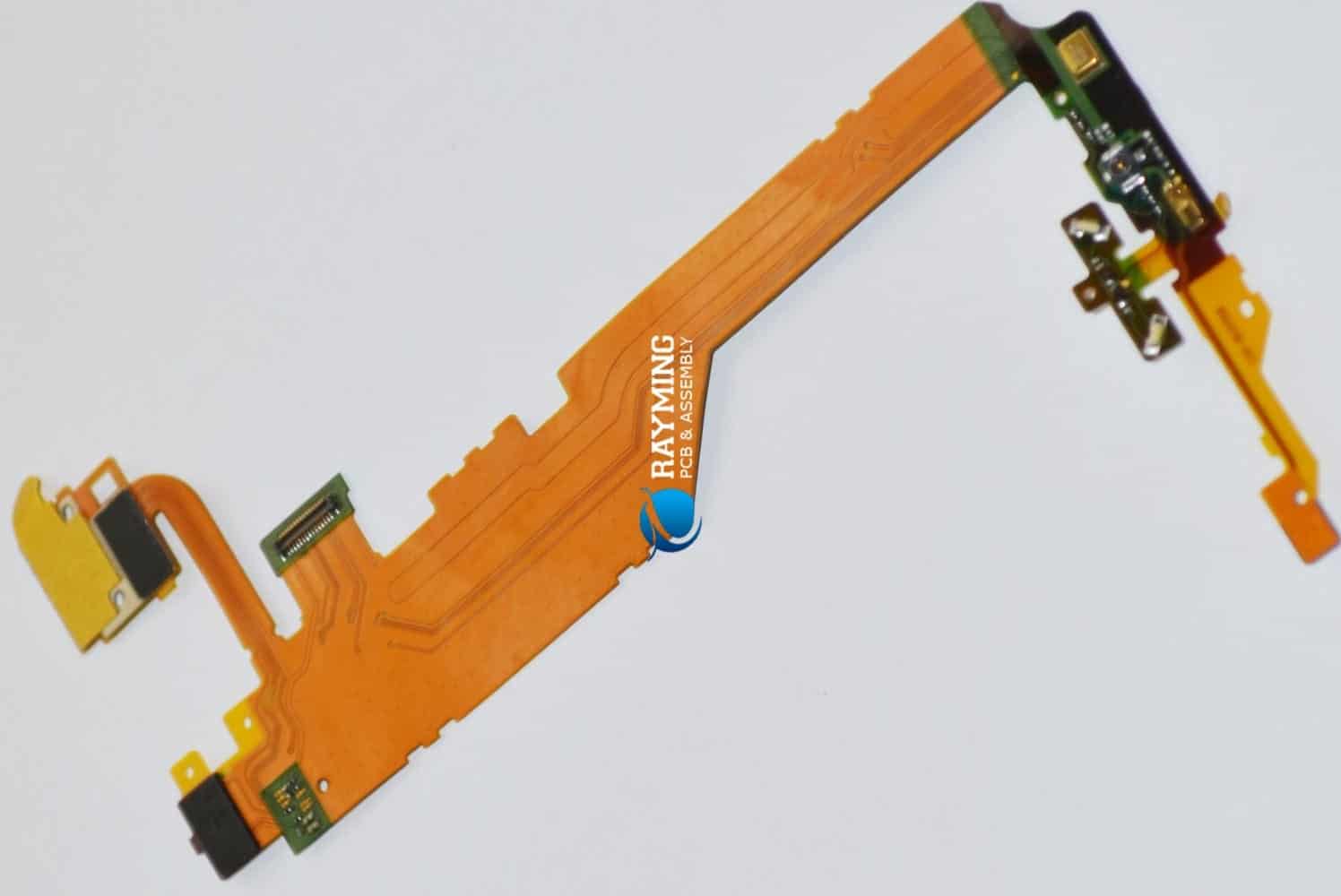
A long flex PCB, also known as a flexible printed circuit board, is a thin and flexible circuit board that allows connections between two or more rigid circuit boards. Long flex PCBs provide various advantages over traditional rigid PCBs, especially in applications that require dynamic flexing, tight space constraints, or three-dimensional routing. This article provides a comprehensive guide on long flex PCB design, manufacturing, and applications.
What is a Long Flex PCB?
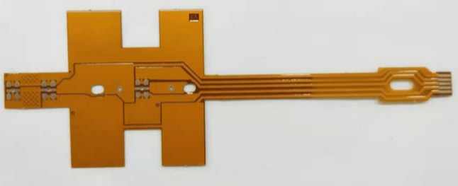
A long flex PCB consists of thin, flexible dielectric layers with conductive tracks printed or etched onto them. The dielectric substrate material is usually polyimide or polyester. Long flex PCBs can be single-sided with tracks on one side, double-sided with tracks on both sides, or multi-layer with multiple conductive layers separated by dielectric.
The flexible nature of long flex PCBs allows them to dynamically flex and bend repeatedly. They can fold into three-dimensional shapes to route between different rigid PCB assemblies. Long flex PCBs are ideal for connecting PCBs that move relative to each other, such as in consumer electronics. They are also well-suited for densely packed electronic devices where space is limited.
Compared to rigid boards, long flex PCBs:
- Are extremely thin and lightweight
- Can bend and twist repeatedly without damage
- Allow three-dimensional routing between PCBs
- Enable compact, space-efficient PCB layouts
- Absorb shock and vibration
- Are low cost for prototyping and low to medium production runs
Long flex PCB lengths can range from a few inches to several feet, with 100mm being a typical minimum length. The maximum length depends on the application but can exceed 3 meters in some cases.
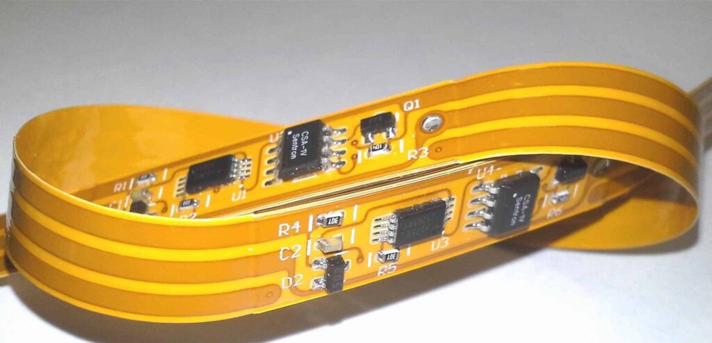
Long Flex PCB Construction
The construction of a long flex PCB involves layers of flexible dielectric material and conductive copper traces. Here are some key elements of the construction:
- Base Dielectric Layer: The base material is typically a polyimide (e.g. Kapton) or polyester (e.g. PET) sheet between 25-100μm thick. Polyimide offers high temperature resistance while PET provides an economical option.
- Conductive Layers: Copper traces are either screen-printed or laminated onto the dielectric layers. Flex PCBs usually have 1-2 conductive layers.
- Coverlay: A polyimide or acrylic coverlay can be laminated over the conductor layers for insulation and protection.
- Stiffeners: Special stiffening materials can be added to create localized rigid sections for connectors or components.
- Cover Coat: An epoxy- or acrylic-based cover coat is applied to protect the copper from oxidation and abrasion.
- Adhesive: Acrylic or epoxy adhesive bonds the layers together providing flexural endurance.
Long Flex PCB Design Considerations
Designing long flex PCBs requires paying attention to flexural stress, impedance, and other factors. Here are some key considerations:
1. Dynamic Flexing and Bends
A primary advantage of long flex PCBs is dynamic flexing. The design should account for the minimum bend radius, number of flex cycles, and any sharp folds. Strain relief cutouts can be added near bends to reduce stress.
2. Layer Stackup
Determine the required number of conductive and dielectric layers. Match dielectric materials to get the thickness, weight, and flexibility needed. Acrylic adhesives maximize flex life.
3. Trace Routing
Use wide traces or copper fills for high current. Route traces perpendicular to the bend axis at flex points. Avoid 90° trace angles. Build test traces to validate trace integrity through dynamic bending.
4. Component Placement
Place sensitive ICs near board stiffeners or the rigid-flex interface. Use flexible adhesives to reinforce component attach. Avoid placing connectors/components at busy dynamic flex areas.
5. Impedance Control
Match trace impedance to desired differential signals. Reference planes above and below traces help control impedance. Vary trace width/space to achieve 100Ω differential impedance.
6. Stiffener Integration
Integrate stiffeners into the flex PCB layers to create rigid sections. Use additional dielectric/copper layers in stiff sections for strength, heat dissipation and fine pitch.
7. ES&D Protection
Add carbon-filled polymer layers to protect against ESD damage during flexing. Protective coatings like nickel/gold also improve corrosion resistance.
8. Test Points
Allow probing test points to validate electrical connectivity andidentify failures. Test coupons can be designed with representative test traces.
9. Panel Utilization
Optimize board outlines on the manufacturing panel to maximize material utilization and control costs. Consider spacing for tooling and fiducials.
10. DFM Practices
Apply standard PCB design for manufacturing checks: no acute angles, sufficient pad sizes, etc. Verify design, layer stackup, and drill drawing.
By considering these design factors, flex PCBs can be optimized for reliability throughout the required dynamic bending cycles.
Long Flex PCB Manufacturing Process
Long flex PCB manufacturing involves specialized processes tailored to flexible boards. The main steps include:
1. Design and Data Preparation
The PCB layout is designed in CAD software. Gerber and drill files are generated. Design rule checks validate manufacturability.
2. Dielectric Material Lamination
Sheets of polyimide or polyester dielectric materials are laminated together using epoxy or acrylic adhesive films.
3. Copper Foil Lamination
Copper foil is laminated onto one or both sides of the dielectric to form the conductive layers.
4. Photolithography
A photoresist is applied on the copper layers. The circuit pattern is exposed and etched to form the conductive traces.
5. Die Cutting
The individual PCB outlines are die cut from the full panel either before or after etching.
6. Component Assembly
Components are attached on the board using soldering or conductive epoxy adhesive.
7. Electrical Testing
Each completed board undergoes in-circuit and functional testing to validate proper performance.
8. Final inspection
Electrical tests, visual inspection, and dimensional checks verify the boards meet specifications.
Flex PCB manufacturers offer quick-turn prototypes through to higher volume production. Choosing an experienced manufacturer is key to getting a reliable, high-quality flex PCB.
Long Flex PCB Applications
The unique properties of long flex PCBs make them suitable for many applications, including:
1. Consumer Electronics
Long flex PCBs connect screens, cameras, buttons, sensors, batteries, and other modules in smartphones, laptops, wearables, and home appliances. Dynamic bending occurs during use.
2. Automotive
Inside automobiles, long flex PCBs connect electronics in doors, dashboards, lighting, engine bays, and other areas. They withstand vibration and repeated movement.
3. Industrial
In robots, machinery, and manufacturing systems, long flex PCBs route signals between moving parts. They also integrate well into space-constrained assemblies.
4. Medical
Long flex PCBs suit body-worn medical devices where a rigid board would be uncomfortable. They allow flexible sensors and interconnects.
5. Military/Aerospace
Rugged flex PCBs withstand shock, vibration, and temperature extremes in defense and aerospace systems while saving weight over traditional wiring harnesses.
With innovations in materials, fabrication, and design, long flex PCBs continue expanding into new and challenging applications where dynamic movement, three-dimensional routing, or space constraints are important.
Flex PCB Design and Manufacturing Q&A
Here are answers to some frequently asked questions about designing and manufacturing long flex PCBs:
Q: What are the minimum and maximum lengths for flex PCBs?
A: Typical minimum lengths are around 100mm (4 inches). Maximum lengths can exceed 3 meters for some applications. Lengths under 150mm tend to be more costly per unit area.
Q: How many conductive layers can flex PCBs support?
A: Most flex PCBs have 1 or 2 conductive layers. Some designs use 4-8 layers, with the dielectric/adhesive thickness increasing. Too many layers impact flexibility.
Q: What are recommended minimum trace/space dimensions?
A: Minimum trace/space is typically 100μm (4 mils) but high-density designs can achieve 50μm (2mil) traces over short distances. Ultra-fine line processes below 25μm are also possible.
Q: What connector types suit flex PCB applications?
A: Common connectors include FPC (flexible printed circuit), FFV (flat flexible cable), and flex-rigid types. Zero insertion force, bottom-contact, and edge-mount styles support high mating cycles.
Q: What type of testability should be designed into flex PCBs?
A: Include testpoints for in-circuit test probes. Use micro-vias or flying probe pads to access traces between layers. Separate test coupon boards validate trace durability through dynamic bending.
Conclusion
With their thin, lightweight, and flexible nature, long flex PCBs provide interconnect solutions not achievable with rigid boards. Careful design consideration must be given to dynamic bending, impedance control, and reliability factors. By partnering with an experienced flex PCB manufacturer, you can develop customized long flex circuits for demanding applications in consumer electronics, automotive, aerospace, medical devices, and more.


Leave a Reply