What is a MOSFET Driver?
A MOSFET (Metal-Oxide-Semiconductor Field-Effect Transistor) driver is an electronic circuit that controls the operation of a MOSFET switch. MOSFETs are widely used in power electronics applications, such as switching power supplies, motor drives, and electronic ballasts. However, driving a MOSFET directly from a microcontroller or other low-power control circuitry can be challenging due to the high gate capacitance and current requirements of the MOSFET.
A MOSFET driver solves this problem by providing the necessary voltage and current to the gate of the MOSFET to turn it on and off efficiently. The driver typically includes a level-shifting circuit to translate the control signals from the logic level (e.g., 3.3V or 5V) to the higher voltage required by the MOSFET gate (e.g., 10V or 12V). It also includes a high-current output stage to rapidly charge and discharge the gate capacitance, enabling fast switching speeds.
Benefits of using a MOSFET driver:
- Faster switching speeds
- Reduced power losses
- Improved reliability
- Simplified control circuitry
Introduction to the IR2104
The IR2104 is a popular high-voltage, high-speed MOSFET driver manufactured by Infineon Technologies (formerly International Rectifier). This driver is designed to control high-side and low-side N-channel MOSFETs in a variety of applications, such as:
- Half-bridge and full-bridge motor drives
- Switching power supplies
- Electronic ballasts
- Automotive electronic controls
Key features of the IR2104:
- High output voltage: up to 600V
- Fast switching speeds: up to 1MHz
- Low-side and high-side output channels
- Bootstrap diode for high-side supply
- Undervoltage lockout protection
- Floating channel for high-side driver

IR2104 Pinout and Pin Description
The IR2104 is available in an 8-pin DIP or SOIC package. The pinout and pin descriptions are as follows:
| Pin Number | Pin Name | Description |
|---|---|---|
| 1 | VCC | Logic supply voltage (10V to 20V) |
| 2 | IN | Logic input for high-side and low-side outputs |
| 3 | COM | Low-side return |
| 4 | LO | Low-side gate drive output |
| 5 | VS | High-side floating supply |
| 6 | VB | High-side bootstrap supply |
| 7 | HO | High-side gate drive output |
| 8 | VDD | Offset voltage for high-side driver (connected to VS) |
Pin functions explained:
VCC (Pin 1)
The VCC pin is the logic supply voltage for the IR2104. It should be connected to a stable voltage source between 10V and 20V. The current draw on this pin is typically less than 1mA.
IN (Pin 2)
The IN pin is the logic input that controls both the high-side and low-side outputs. A logic high (>2.2V) on this pin will turn on the high-side MOSFET and turn off the low-side MOSFET. A logic low (<0.8V) will have the opposite effect.
COM (Pin 3)
The COM pin is the low-side return path for the driver. It should be connected to the source of the low-side MOSFET and the negative rail of the power supply.
LO (Pin 4)
The LO pin is the low-side gate drive output. It provides the necessary voltage and current to drive the gate of the low-side MOSFET. When the IN pin is low, the LO output will be pulled up to VCC to turn on the low-side MOSFET. When IN is high, LO will be pulled down to COM to turn off the low-side MOSFET.
VS (Pin 5)
The VS pin is the high-side floating supply. It provides the reference voltage for the high-side driver and should be connected to the source of the high-side MOSFET. The voltage on this pin can float up to 600V with respect to COM.
VB (Pin 6)
The VB pin is the bootstrap supply for the high-side driver. It should be connected to a capacitor (bootstrap capacitor) that is charged to VCC when the low-side MOSFET is on. This capacitor provides the necessary voltage to drive the high-side MOSFET when it is turned on.
HO (Pin 7)
The HO pin is the high-side gate drive output. It provides the voltage and current to drive the gate of the high-side MOSFET. When the IN pin is high, the HO output will be pulled up to VB to turn on the high-side MOSFET. When IN is low, HO will be pulled down to VS to turn off the high-side MOSFET.
VDD (Pin 8)
The VDD pin is connected to the VS pin to provide an offset voltage for the high-side driver. This connection is necessary for the proper operation of the high-side floating supply.

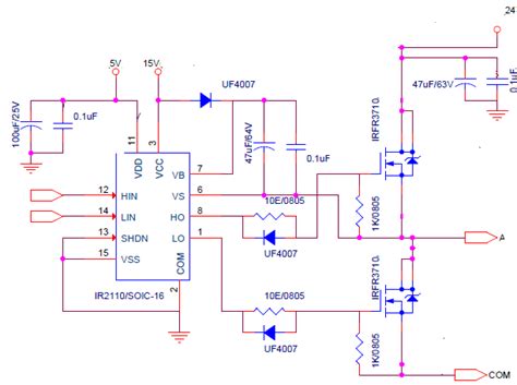
IR2104 Typical Application Circuit
A typical application circuit for the IR2104 in a half-bridge configuration is shown below:
                              VCC
                               |
                              +-+
                              | |
                              | |  IR2104
                              | |
                              | |  VB   HO
                              | +--+--|>|--+--------+
                              |    |       |        |
                              |    +-------+        |
                              |    |              /\/\/\
                              |    |              |    |
                              |    |              +----+
                              |    |              |    |
            PWM Input         |    |              |    |  High-Side
            +-----------------|----+              |    |  MOSFET
            |                 |  VS|              +----+
            |                 |    |                |
            |                 +----+                |
            |                 |    |                |
            |          IN     |    |                |
            +-----------------|--+ |                |
                              |  | |                |
                              |  +-+                |
                              |  COM                |
                              |    |                |
                              |    +----------------+
                              |    |
                              |    |
                              |    |
                              |    |  Low-Side
                              |    |  MOSFET
                              |    |
                              |   /\/\/\
                              |    |
                              +----+
                                   |
                                  GND
In this circuit:
- The VCC pin is connected to a 12V supply.
- The IN pin is driven by a PWM signal from a microcontroller or other control circuitry.
- The COM pin is connected to the source of the low-side MOSFET and ground.
- The LO pin drives the gate of the low-side MOSFET.
- The VS pin is connected to the source of the high-side MOSFET.
- The VB pin is connected to a bootstrap capacitor, which is charged to 12V when the low-side MOSFET is on.
- The HO pin drives the gate of the high-side MOSFET.
- The VDD pin is connected to the VS pin.

IR2104 Bootstrap Circuit Operation
The bootstrap circuit is a key feature of the IR2104 that enables it to drive the high-side MOSFET in a half-bridge configuration. The bootstrap capacitor is charged to the VCC voltage when the low-side MOSFET is on, and it provides the necessary voltage to drive the high-side MOSFET when it is turned on.
The operation of the bootstrap circuit can be divided into two phases:
- Charging phase (low-side MOSFET on)
- Discharging phase (high-side MOSFET on)
Charging phase:
During the charging phase, the low-side MOSFET is turned on, and the high-side MOSFET is turned off. The VS pin is pulled down to ground, and the bootstrap capacitor is charged to the VCC voltage through the bootstrap diode (internal to the IR2104).
The charging current for the bootstrap capacitor flows from VCC, through the bootstrap diode, and into the capacitor. The capacitor voltage will rise to VCC – Vf, where Vf is the forward voltage drop of the bootstrap diode (typically 0.7V).
Discharging phase:
During the discharging phase, the high-side MOSFET is turned on, and the low-side MOSFET is turned off. The VS pin rises to the high-side supply voltage, and the VB pin follows, maintaining a voltage of VCC – Vf above VS.
The bootstrap capacitor now serves as the floating supply for the high-side driver, providing the necessary voltage to turn on the high-side MOSFET. The capacitor starts to discharge through the high-side MOSFET gate and the HO pin.
The discharging phase continues until the high-side MOSFET is turned off, and the low-side MOSFET is turned on again, restarting the charging phase.
Sizing the bootstrap capacitor:
The size of the bootstrap capacitor is an important consideration in the design of an IR2104-based circuit. The capacitor must be large enough to supply the required gate charge for the high-side MOSFET without excessive voltage droop, but not so large that it takes too long to charge during the charging phase.
A general rule of thumb is to size the bootstrap capacitor according to the following equation:
C_boot >= 10 * Q_g / V_droop
Where:
– C_boot is the bootstrap capacitor value in farads (F)
– Q_g is the total gate charge of the high-side MOSFET in coulombs (C)
– V_droop is the maximum allowable voltage droop on the VB pin (typically 0.1V to 0.2V)
For example, if the high-side MOSFET has a total gate charge of 50nC and the maximum allowable voltage droop is 0.2V, the minimum bootstrap capacitor value would be:
C_boot >= 10 * 50nC / 0.2V = 2.5uF
In practice, a larger capacitor value (e.g., 4.7uF or 10uF) is often used to provide a safety margin and ensure reliable operation over a wide range of conditions.
IR2104 Deadtime Control
Deadtime is the period during which both the high-side and low-side MOSFETs are turned off to prevent shoot-through currents. Shoot-through occurs when both MOSFETs are on simultaneously, creating a short circuit between the high-side and low-side supply rails. This can result in excessive current draw, increased power dissipation, and potentially damage the MOSFETs or other components.
The IR2104 does not include built-in deadtime control, so it must be implemented externally using the control circuitry (e.g., a microcontroller or FPGA) that drives the IN pin.
Implementing deadtime control:
To implement deadtime control, the control circuitry should insert a short delay between turning off one MOSFET and turning on the other. This delay should be long enough to ensure that the first MOSFET has fully turned off before the second MOSFET starts to turn on.
The required deadtime depends on several factors, including:
- The turn-off time of the MOSFETs
- The propagation delay of the IR2104
- The gate resistance and capacitance of the MOSFETs
- The layout and parasitics of the PCB
A typical deadtime value for an IR2104-based circuit is in the range of 100ns to 1us. The deadtime can be generated using software delays, hardware timers, or dedicated deadtime generation circuits.
Deadtime insertion methods:
There are two common methods for inserting deadtime in an IR2104-based circuit:
- Pulse-Width Modulation (PWM) with deadtime
- Complementary PWM with deadtime
PWM with deadtime:
In this method, the control circuitry generates a single PWM signal with the desired deadtime inserted between the high-side and low-side pulses. The PWM signal is connected to the IN pin of the IR2104, which drives the high-side and low-side MOSFETs accordingly.
The advantage of this method is that it requires only a single PWM output from the control circuitry. However, it may be more challenging to generate the PWM signal with the desired deadtime, especially if the control circuitry has limited resolution or flexibility.
Complementary PWM with deadtime:
In this method, the control circuitry generates two complementary PWM signals, one for the high-side MOSFET and one for the low-side MOSFET. The deadtime is inserted by delaying the rising edge of each PWM signal relative to the falling edge of the other.
The two PWM signals are then combined using an AND gate or a similar logic function, and the resulting signal is connected to the IN pin of the IR2104.
The advantage of this method is that it allows for more precise control of the deadtime, as each PWM signal can be generated independently. However, it requires two PWM outputs from the control circuitry and additional external logic to combine the signals.
IR2104 PCB Layout Considerations
Proper PCB layout is crucial for the optimal performance and reliability of an IR2104-based circuit. The high-speed switching and high-voltage operation of the MOSFETs can result in significant electromagnetic interference (EMI) and voltage transients if the layout is not carefully designed.
Here are some key PCB layout considerations for an IR2104-based circuit:
Component placement:
- Place the IR2104 as close as possible to the MOSFETs to minimize the length of the gate drive traces.
- Place the bootstrap capacitor as close as possible to the VB and VS pins of the IR2104.
- Place the input and output capacitors close to the MOSFETs to minimize the loop area and reduce EMI.
Trace routing:
- Use wide, short traces for the high-current paths (e.g., the MOSFET drain and source connections).
- Use a ground plane to provide a low-impedance return path for the high-frequency currents.
- Route the gate drive traces (HO and LO) away from the high-current traces to avoid coupling and EMI.
- Keep the gate drive traces as short and straight as possible to minimize inductance and ringing.
Power planes:
- Use separate power planes for the high-side and low-side supplies to reduce coupling and noise.
- Use a continuous ground plane to provide shielding and reduce EMI.
Isolation:
- Provide adequate clearance and creepage distance between the high-voltage and low-voltage sections of the board to prevent arcing and insulation breakdown.
- Use isolation techniques (e.g., optocouplers or transformers) to isolate the control circuitry from the high-voltage section if necessary.
IR2104 Protection Features
The IR2104 includes several built-in protection features to ensure reliable operation and prevent damage to the MOSFETs and other components in the circuit.
Undervoltage lockout (UVLO):
The IR2104 includes an undervoltage lockout (UVLO) circuit that disables the output drivers if the VCC voltage falls below a certain threshold (typically 8.2V). This prevents the MOSFETs from operating in an undefined state or with insufficient gate drive voltage, which could result in excessive power dissipation or damage.
The UVLO circuit has a hysteresis of typically 500mV to prevent oscillation and ensure clean transitions between the on and off states.
Floating channel:
The IR2104 includes a floating channel for the high-side driver, which allows it to operate with a high-side supply voltage up to 600V above the COM pin voltage. This is achieved using the bootstrap circuit and the high-voltage level-shifting circuitry internal to the IR2104.
The floating channel eliminates the need for a separate high-side power supply or an isolation transformer, simplifying the circuit design and reducing cost.
Shoot-through prevention:
Although the IR2104 does not include built-in deadtime control, its output drivers are designed to prevent shoot-through currents by ensuring that the high-side and low-side MOSFETs are never turned on simultaneously.
The IR2104 achieves this by using a proprietary output driver design that provides a high-impedance state between the HO and LO outputs during transitions, preventing any overlap between the gate drive signals.
However, as mentioned earlier, external deadtime control is still recommended to provide an additional layer of protection and ensure reliable operation over a wide range of conditions.
IR2104 Applications
The IR2104 is a versatile MOSFET driver that can be used in a wide range of applications, including:
Half-bridge and full-bridge motor drives:
The IR2104 is well-suited for driving the high-side and low-side MOSFE


Leave a Reply