What is Soldermask and Why is Exposure Important?
Soldermask, also known as solder resist or solder mask, is a thin layer of polymer applied to the copper traces of a printed circuit board (PCB). Its primary functions are to:
- Protect the copper traces from oxidation and corrosion
- Prevent solder from bridging between traces during assembly
- Provide electrical insulation between conductive parts
- Improve the aesthetics and readability of the PCB
Proper exposure of the soldermask is crucial for ensuring its effectiveness in serving these functions. Underexposed soldermask may not fully cure or adhere properly to the PCB surface, leading to inadequate protection and potential issues during assembly. Overexposure can cause the soldermask to become brittle, crack, or peel off the PCB.
Soldermask Composition
Soldermask is typically composed of:
| Component | Function |
|---|---|
| Resin | Forms the base material and provides adhesion |
| Photoinitiators | Initiate polymerization upon exposure to UV light |
| Fillers | Enhance mechanical and thermal properties |
| Pigments | Provide color (green, blue, red, black, etc.) |
| Additives | Improve flow, leveling, and other characteristics |
The specific composition varies depending on the soldermask type (liquid photoimageable, dry film, or liquid photoimageable dry film) and the manufacturer.
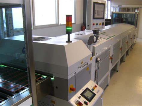
Soldermask Exposure Methods
There are two primary methods for exposing soldermask during PCB production:
- Photolithography (most common)
- Direct imaging
Photolithography
Photolithography involves the use of a phototool (also called a photomask) to selectively expose the soldermask to UV light. The process typically follows these steps:
- Soldermask Application: The soldermask is applied to the PCB surface by either:
- Curtain coating or screen printing for liquid photoimageable soldermask
-
Lamination for dry film soldermask
-
Pre-exposure Bake: The PCB is heated to remove solvents and improve adhesion.
-
Exposure: The phototool is placed on top of the soldermask-coated PCB, and UV light is shone through the clear areas of the phototool. This causes the photoinitiators in the exposed areas to begin polymerization.
-
Development: The unexposed areas of the soldermask are removed using a developer solution, leaving behind the desired soldermask pattern.
-
Post-exposure Bake: The PCB is heated again to fully cure the remaining soldermask and improve its mechanical and chemical properties.
Phototool Considerations
The quality and accuracy of the phototool are critical for achieving proper soldermask exposure. Factors to consider include:
-
Material: Phototools can be made from film or glass. Film is less expensive but more prone to dimensional changes and damage. Glass offers higher stability and resolution but is more costly.
-
Emulsion: The emulsion side of the phototool should face the soldermask to minimize undercutting and maintain feature accuracy.
-
Alignment: The phototool must be properly aligned with the PCB features to ensure correct registration of the soldermask pattern.
-
Optical Density: A high optical density (>4.0) is desirable to maximize contrast and minimize UV light bleed-through in the dark areas of the phototool.
Direct Imaging
Direct imaging eliminates the need for a phototool by using a laser or UV LED to directly expose the soldermask in the desired pattern. The process is similar to photolithography, but the exposure step is performed using a computer-controlled imaging system instead of a phototool.
Advantages of direct imaging include:
- Reduced setup time and cost by eliminating phototool production
- Improved registration and feature accuracy
- Faster turnaround times for design changes
- Increased yield due to fewer defects caused by phototool misalignment or damage
However, direct imaging systems have a higher initial cost and may require more specialized operator training compared to photolithography.

Factors Affecting Soldermask Exposure
Several factors can influence the quality and consistency of soldermask exposure, including:
UV Light Intensity and Spectrum
The UV light source must provide sufficient intensity and the appropriate wavelength range to efficiently initiate polymerization in the soldermask. Common UV light sources include:
- Mercury vapor lamps
- Metal halide lamps
- UV LED arrays
The optimal wavelength range for soldermask exposure is typically between 350-400 nm. Light intensity should be regularly monitored and maintained within the soldermask manufacturer’s recommended range to ensure consistent exposure results.
Exposure Time
Exposure time directly affects the depth and degree of soldermask polymerization. Insufficient exposure time can lead to incomplete curing and poor adhesion, while excessive exposure can cause brittleness and cracking.
The optimal exposure time depends on factors such as:
- Soldermask type and thickness
- UV light intensity and spectrum
- Desired soldermask properties
Exposure time should be determined through testing and consultation with the soldermask manufacturer, then carefully controlled during production.
Soldermask Thickness
Soldermask thickness plays a role in determining the required exposure time and the final properties of the cured soldermask. Thicker soldermask layers require longer exposure times to ensure complete polymerization through the entire depth of the material.
Typical soldermask thicknesses range from 0.5-2.0 mils (12.7-50.8 microns), with the specific target thickness depending on the PCB design and application requirements.
Temperature and Humidity
Ambient temperature and humidity can affect soldermask exposure and development processes. High humidity can cause the soldermask to absorb moisture, leading to reduced adhesion and potential defects. Elevated temperatures can accelerate the polymerization reaction, shortening the required exposure time.
To minimize these effects, soldermask exposure should be performed in a controlled environment with stable temperature and humidity levels. Recommended conditions are typically:
- Temperature: 68-77°F (20-25°C)
- Relative Humidity: 40-60%

Optimizing Soldermask Exposure
Achieving consistent, high-quality soldermask exposure requires careful process control and optimization. Key steps include:
- Soldermask Selection: Choose a soldermask that is compatible with your PCB design, assembly process, and end-use requirements. Consider factors such as:
- Soldermask type (liquid photoimageable, dry film, or liquid photoimageable dry film)
- Thickness
- Color
- Electrical and mechanical properties
- Chemical resistance
-
Thermal stability
-
Equipment Calibration: Regularly calibrate and maintain exposure equipment to ensure consistent UV light intensity and spectrum. This includes:
- Replacing UV lamps at recommended intervals
- Cleaning optical components
- Checking and adjusting alignment mechanisms
-
Verifying exposure time and intensity settings
-
Process Parameter Optimization: Conduct testing to determine the optimal process parameters for your specific soldermask and PCB design. Key parameters to optimize include:
- Exposure time
- Developing time and solution concentration
- Pre- and post-exposure bake temperatures and times
-
Soldermask application method and thickness
-
Quality Control: Implement a robust quality control program to monitor soldermask exposure consistency and identify potential issues early. This may include:
- Visual inspection of soldermask coverage and alignment
- Thickness measurements
- Adhesion testing
- Electrical insulation resistance testing
- Microsectioning to verify complete polymerization
By following these guidelines and continually refining your soldermask exposure process, you can ensure reliable PCB Protection and performance.

Frequently Asked Questions (FAQ)
1. What is the difference between liquid photoimageable and dry film soldermask?
Liquid photoimageable soldermask is applied to the PCB surface in liquid form by curtain coating or screen printing, then exposed and developed. Dry film soldermask is a solid film that is laminated onto the PCB surface before exposure and development. Liquid photoimageable soldermask offers better conformity to surface features and finer resolution, while dry film soldermask provides more consistent thickness control and is less sensitive to environmental conditions.
2. Can soldermask be exposed using a standard UV light source?
While soldermask can be exposed using a standard UV light source, it is recommended to use a dedicated exposure system with a UV light source specifically designed for soldermask exposure. These systems provide the optimal UV wavelength range and intensity for efficiently initiating polymerization in the soldermask material.
3. How do I determine the appropriate soldermask thickness for my PCB?
The appropriate soldermask thickness depends on factors such as the PCB design, component types, and end-use requirements. Thinner soldermask layers (0.5-1.0 mils) are typically used for fine-pitch components and high-density designs, while thicker layers (1.0-2.0 mils) provide better protection and insulation for larger components and higher voltage applications. Consult with your PCB manufacturer and soldermask supplier to determine the optimal thickness for your specific needs.
4. What causes soldermask to peel or crack after exposure?
Soldermask peeling or cracking can be caused by several factors, including:
– Overexposure, leading to brittleness
– Poor adhesion due to surface contamination or inadequate pre-exposure baking
– Mechanical stress during handling or thermal cycling
– Incompatibility between the soldermask and PCB surface materials
To prevent these issues, ensure proper surface preparation, follow the manufacturer’s recommended exposure and baking parameters, and handle the PCBs with care during processing and assembly.
5. Can soldermask exposure be performed in a non-cleanroom environment?
While soldermask exposure can be performed in a non-cleanroom environment, it is recommended to do so in a controlled area with filtered air and stable temperature and humidity levels. Dust, dirt, and other contaminants can cause defects in the exposed soldermask pattern, while fluctuations in temperature and humidity can affect the exposure and development processes. If a full cleanroom is not available, consider using a dedicated exposure room with environmental controls to minimize potential issues.


Leave a Reply