What is an HDI PCB Stackup?
An HDI PCB stackup refers to the arrangement of copper layers, dielectric materials, and vias within a printed circuit board. The stackup defines the electrical properties, signal integrity, and physical characteristics of the PCB. In HDI PCBs, the stackup typically involves more layers and smaller features compared to traditional PCBs, enabling higher density and improved performance.
Types of HDI PCB Stackups
There are several types of HDI PCB stackups, each with its own advantages and considerations. Let’s take a closer look at the most common ones:
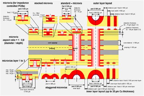
1. Microvia Stackup
Microvia stackups utilize small, laser-drilled vias with diameters less than 150 microns. These vias are typically used to connect the outer layers to the inner layers of the PCB. Microvia stackups offer several benefits:
- Increased routing density
- Improved signal integrity
- Reduced layer count
- Smaller form factors
However, microvia stackups also come with some challenges, such as:
- Higher manufacturing costs
- Increased complexity in design and fabrication
- Potential reliability issues if not designed properly
2. Buried Via Stackup
Buried via stackups involve vias that are placed between the inner layers of the PCB and do not extend to the outer layers. This type of stackup offers several advantages:
- Reduced via count on the outer layers
- Improved signal integrity
- Increased routing space on the outer layers
However, buried via stackups also have some drawbacks:
- Higher manufacturing costs compared to traditional through-hole vias
- Increased complexity in design and fabrication
- Potential signal integrity issues if not designed properly
3. Hybrid Stackup
Hybrid stackups combine both microvia and buried via technologies to achieve the best of both worlds. This type of stackup offers:
- High routing density
- Excellent signal integrity
- Flexibility in design and layout
However, hybrid stackups also come with some challenges:
- Higher manufacturing costs due to the combination of technologies
- Increased complexity in design and fabrication
- Potential reliability issues if not designed properly

Choosing the Right HDI PCB Stackup for YRAYPCB
When selecting the appropriate HDI PCB stackup for your YRAYPCB project, there are several factors to consider:
-
Electrical Requirements: Consider the signal speed, frequency, and impedance requirements of your design. Choose a stackup that can support these requirements while maintaining signal integrity.
-
Mechanical Requirements: Take into account the physical dimensions, thickness, and weight constraints of your PCB. Ensure that the chosen stackup can accommodate these requirements.
-
Manufacturing Capabilities: Evaluate the manufacturing capabilities of your PCB fabricator. Make sure they have the necessary equipment, expertise, and experience to produce the desired stackup reliably and cost-effectively.
-
Cost Considerations: Compare the costs associated with different stackup options. While HDI PCBs generally have higher manufacturing costs compared to traditional PCBs, the right stackup choice can help optimize the cost-performance balance.
-
Reliability and Durability: Consider the operating environment and expected lifecycle of your product. Choose a stackup that can withstand the anticipated stresses and maintain reliable performance over the desired lifespan.
To help visualize the different HDI PCB stackup options, refer to the following table:
| Stackup Type | Layers | Microvia | Buried Via | Hybrid |
|---|---|---|---|---|
| 1+N+1 | 4-6 | Yes | No | No |
| 2+N+2 | 6-8 | Yes | Yes | No |
| 3+N+3 | 8-10 | Yes | Yes | Yes |
| 4+N+4 | 10-12 | Yes | Yes | Yes |
*N represents the number of inner layers in the stackup.

Frequently Asked Questions (FAQ)
-
Q: What is the difference between an HDI PCB and a traditional PCB?
A: HDI PCBs have higher routing density, smaller features, and more complex stackups compared to traditional PCBs. They enable more functionality in smaller form factors and offer improved signal integrity. -
Q: How do I determine the number of layers needed for my HDI PCB?
A: The number of layers required depends on factors such as the complexity of your design, signal requirements, and available space. Work with your PCB design team and fabricator to determine the optimal layer count for your specific project. -
Q: Can I mix different via types in the same HDI PCB stackup?
A: Yes, hybrid stackups allow for the combination of microvia and buried via technologies in the same PCB. This offers flexibility in design and can help optimize performance and manufacturability. -
Q: Are HDI PCBs more expensive than traditional PCBs?
A: Yes, HDI PCBs generally have higher manufacturing costs due to the advanced technologies and processes involved. However, the increased functionality and performance benefits often justify the added cost. -
Q: How can I ensure the reliability of my HDI PCB?
A: To ensure reliability, follow best design practices, select high-quality materials, and work with an experienced PCB fabricator. Conduct thorough testing and validation to identify and address any potential issues early in the development process.

Conclusion
Choosing the right HDI PCB stackup is essential for achieving optimal performance, reliability, and manufacturability in your YRAYPCB project. By understanding the different stackup types and considering factors such as electrical requirements, mechanical constraints, manufacturing capabilities, cost, and reliability, you can make an informed decision that best suits your specific needs.
Remember to collaborate closely with your PCB design team and fabricator throughout the process to ensure a successful outcome. With the right HDI PCB stackup, you can unlock the full potential of your electronic device and stay ahead in today’s competitive market.


Leave a Reply