Introduction to Flex Circuits
Flexible printed circuit boards (flex circuits or flex PCBs) are a type of printed circuit board made using flexible substrate materials like polyimide or polyester. Unlike traditional rigid PCBs, flex circuits can bend and flex to fit into tight or moving spaces in electronic devices. They are commonly used when electronics need to mount on irregular or dynamic surfaces, in wearable devices, or in dynamic flexing applications like robotic arms or avionics. Flex circuits allow complex interconnectivity while conforming around joints or in three-dimensional configurations.
Flex PCBs offer many benefits compared to rigid boards:
- Greater flexibility and ability to conform to dynamic shapes
- Thinner, lightweight, and compact for smaller devices
- High connectivity density with fine traces and spacing
- Reduced wiring and simplified assembly
- Improved reliability with dynamic flexing motions
- Design innovation opportunities in 3D and wearable tech
However, flex circuit design comes with its own set of challenges and considerations for PCB designers and engineers:
Key Design Challenges for Flex PCBs
- Choosing optimal flexible materials
- Minimizing flex cracks with dynamic bending
- Maintaining trace integrity over flex zones
- Managing thermal stresses
- Handling high-density interconnects
- Addressing EMI shielding needs
- Withstanding environmental exposures
- Providing sufficient stiffness for assembly
This guide will provide a comprehensive overview of flex circuit design, materials, construction, modeling, analysis, and assembly considerations for developing robust flexible PCBs.
Flexible Substrate Materials
Choosing the right flexible material system is one of the most critical aspects in designing a successful flex circuit. The substrate material defines the flex circuit’s fundamental mechanical, electrical, and environmental capabilities. Key properties to evaluate when selecting materials include:
Flexibility
The flexural modulus determines the substrate’s inherent flexible properties. Lower modulus values indicate more flexible, easily bendable materials. Typical flex circuit materials have a flexural modulus between 0.3-10 GPa.
Dielectric Constant
The dielectric constant affects signal propagation speed, impedance, and crosstalk. Most flex circuit materials have a dielectric constant between 3-4.
Loss Tangent
The loss tangent indicates the dielectric loss and attenuation of high frequency signals. Lower loss tangent values minimize signal loss. Common values range from 0.002-0.025.
Thermal Properties
The thermal expansion coefficient affects reliability with temperature changes. The glass transition temperature indicates maximum application temperatures before mechanical changes occur.
Environmental Resistance
Important environmental factors to consider include moisture absorption, flammability, chemical resistance, and UV/weathering stability.
Thickness
Thinner materials allow tighter bend radii but impact stiffness and handling. Standard thicknesses range from 25-100 microns.
| Material | Flexural Modulus (GPa) | Dielectric Constant | Loss Tangent | Thickness (μm) |
|---|---|---|---|---|
| Polyimide | 2-5 | 3.2-3.5 | 0.002-0.010 | 25-100 |
| Polyester | 2-5 | 3.0-3.2 | 0.015-0.018 | 25-125 |
| LCP | 5-10 | 3.1-3.2 | 0.003-0.005 | 25-100 |
Polyimide films like Kapton HN are most commonly used due to their excellent flexibility, electrical performance, and thermal stability. However, polyester and liquid crystal polymer (LCP) films are also popular options. The substrate choice depends on balancing flexural, electrical, and reliability needs.
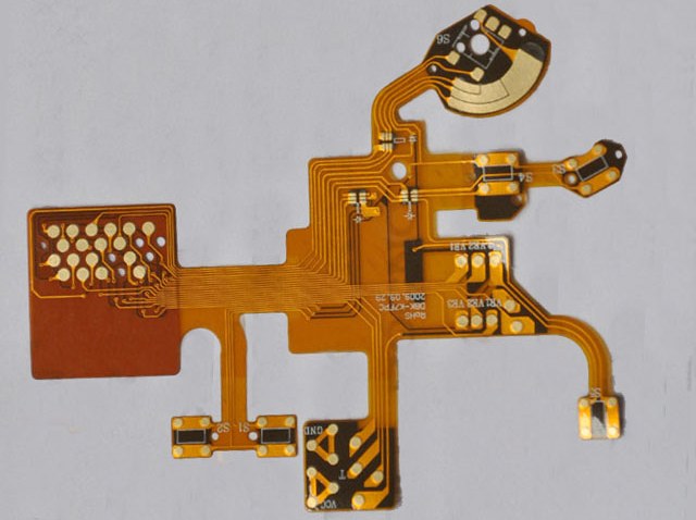
Flex Circuit Construction
Flex circuits consists of multiple layers of flexible substrate with conductive traces and features on one or both sides. Here are the basic construction elements:
Base Material
The flex circuit base is the core flexible dielectric film. Polyimide is most often used. Required thickness depends on manufacturing capabilities, stiffness needs, and flexibility requirements.
Conductive Traces
Usually copper traces are patterned on the polyimide base layer through additive, subtractive, or semi-additive metallization processes. Traces transmit signals and power.
Dielectric Coverlayer
A thin polyimide coverlayer is laminated over the copper to prevent shorts and environmental damage. Openings in the coverlayer provide testpoints and component access.
Stiffeners
To aid assembly and installation, additional polyimide or metal stiffeners are often added in select areas to provide strength and stability.
Adhesives
Acrylic or epoxy adhesives attach coverlayers, stiffeners, and components onto the flexible circuit layers.
Finishes and Coatings
Special finishes like ENIG, immersion silver, or solder mask are applied to protect and facilitate soldering.
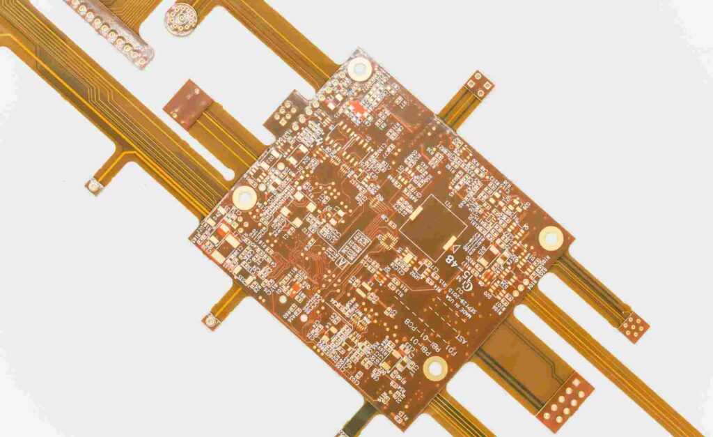
With this basic construction, flex circuits can be designed with single or double-sided traces, multilayer circuits with complex interconnects, and mixed rigid-flex configurations.
Flex Circuit Layout Considerations

Designing the physical layout and routing for a flex circuit requires special considerations across the flexible regions. Here are key guidelines for flex circuit layouts:
Bend Radii
A minimum bend radius must be maintained to avoid overstress and premature cracking. Typical flex materials allow bending to a minimum inside radius of 5-10 times the substrate thickness. For 50 micron polyimide, at least a 2.5mm radius would be recommended.
Flex Bend Areas
Conductive traces will fracture if flexed excessively so plan circuit routing to avoid traces crossing bending zones. Place flexible regions selectively between rigid areas.
Trace Width and Spacing
Use larger trace widths and spacing when crossing flexible areas to account for distortions. Aim for at least 150 micron lines/spaces.
Trace Routing Angles
Avoid acute trace angles less than 30° across flex areas. Gradual curved traces withstand flexing much better than traces at sharp angles.
Annular Rings
Sufficient pad diameters and annular rings are essential for solder joint reliability. 50 mil pad diameters with 4-5 mil annular rings are typical.
Cross-hatching
Added cross-hatched copper balances stresses and prevents confirmation distortions over bending areas.
Stiffeners and Supports
Strategically placed stiffeners maintain stability for assembly and installation while allowing dynamic flexing only in designated zones.
Modeling and Analysis of Flex Circuits
Validating the reliability of flexible PCBs requires advanced modeling, simulation, and analysis with specialized tools. Important analyses to perform include:
Mechanical Stress Analysis
Finite element analysis predicts stresses and deformation over bending regions. This ensures trace integrity is maintained without overstressing materials.
Thermal Simulation
Thermal modeling analyzes temperature gradients and heat dissipation needs. This avoids flex circuit damage or failure from excessive heat during operation.
Vibration and Fatigue Analysis
Vibration analysis determines resonant modes and assesses fatigue life with repetitive dynamic bending stresses.
Drop Impact Testing
Simulating drop events validates robustness against sudden impacts during use.
Impedance Modeling
Transmission line modeling verifies matched impedance for high speed signals across flex regions.
With advanced simulations, engineers can optimize flex circuit constructions and trace routing to withstand mechanical, thermal, vibration, shock, and electrical stresses across real-world operating conditions.
Assembly and Manufacturing Processes
Specialized assembly and soldering processes are required to produce and populate flex circuits without damage.
Fabrication
Photolithographic processes precisely pattern copper traces and features onto flex substrates. Thin, lightweight materials are more challenging to handle than rigid boards during processing.
Layer Alignment
Maintaining layer-to-layer registration and trace alignment is critical, especially for multilayer flex circuits. Misalignments create defects.
Via Forming
Precisely formed microvias generate vertical interconnects between flex circuit layers. Reliable connections are essential.
Attachment
Parts are often assembled onto flex circuits through solder, conductive adhesive, or thermosonic bonding rather than insertion or press-fit.
Soldering
Reflow soldering operations require optimized temperature profiles, preheating, and cooling rates to avoid damage, warping, or delamination.
Rework
Repairs, modifications, and rework are challenging on fragile flex boards. Specially designed tweezer tools manipulate these boards without damage.
With rigorous process engineering controls, flex circuits can be fabricated and assembled to high yields and reliable quality standards.
Applications and Examples
Some examples of how flex circuits are transforming electronics:
Wearable Technology
In smartwatches and fitness bands, flex circuits conform comfortably to the wrist while allowing dynamic movements.
Mobile Devices
Phones and tablets use flex circuits for interconnectivity around hinged, folded, or sliding mechanisms.
Automotive Electronics
Flex circuits mount dashboard displays and enable steering wheel controls that can be positioned ergonomically.
Medical Devices
In hearing aids, prosthetics, and implants, flex circuits reliably fit into tiny spaces while enabling complex functionality.
Robotics and UAVs
Flexible circuits withstand millions of bending cycles in robotic arms. They also save weight and space in drone designs.
Consumer Electronics
Foldable laptops, flexible displays, and dynamic IoT products integrate flex circuits for innovation opportunities.
FAQ
What are the main benefits of using flex circuits?
The main benefits are increased flexibility and conformability, lighter weight and smaller size, simplified cabling and assembly, increased reliability in dynamic applications, and expanded design options for innovative form factors and movement.
How small can flex circuit traces and spaces be?
With advanced processes, trace widths and spaces approaching 50 microns are achievable. However, 150+ micron features are recommended for reliability across flex zones. Narrow 25 micron lines can be used in rigid regions.
Can components be mounted directly onto flex circuits?
Yes, components can be soldered or adhesively attached. However, the thin, lightweight nature of flex circuits means large or heavy components may require additional stiffeners, support structures, or specific mounting arrangements.
What limits the bend radius of a flex circuit?
The flex circuit’s minimum bend radius is limited by the substrate material’s flexural modulus, ductility, and thickness. Typical flex circuit materials allow a minimum inside bend radius of 5 to 10 times the substrate thickness before mechanical failure occurs.
How many flex cycles can a flex circuit withstand?
Properly designed flex circuits can achieve several million flex cycles before fatigue failure, but this depends significantly on the materials, trace routing, dynamic bending stresses, and other factors. Extensive modeling, testing, and qualification over expected conditions is required.
Summary
Flex circuits enable innovative electronics with their ability to dynamically flex and conform. However, realizing the benefits of flex PCBs requires advanced materials selection, layout strategies, modeling tools, assembly processes, and rigorous reliability testing. With sound engineering disciplines, flex circuits can withstand millions of flex cycles and empower the next generation of flexible, wearable, and compact electronics. This guide provides PCB designers and engineers an in-depth overview of best practices for developing robust flex circuits.


Leave a Reply