What is a Semiconductor?
A semiconductor is a material that has electrical conductivity between that of an insulator and a conductor. Its ability to conduct electricity can be controlled through various means, such as doping, temperature, and exposure to light. This unique property makes semiconductors the foundation of modern electronics.
Types of Semiconductors
There are two main types of semiconductors:
-
Intrinsic Semiconductors: These are pure semiconductors without any added impurities. Examples include silicon (Si) and germanium (Ge).
-
Extrinsic Semiconductors: These are semiconductors that have been doped with impurities to modify their electrical properties. There are two types of extrinsic semiconductors:
- N-type: Doped with elements that have more valence electrons than the semiconductor, such as phosphorus (P) or arsenic (As).
- P-type: Doped with elements that have fewer valence electrons than the semiconductor, such as boron (B) or gallium (Ga).
Semiconductor Materials
While silicon is the most widely used semiconductor material, there are several others with unique properties that make them suitable for specific applications:
| Material | Properties | Applications |
|---|---|---|
| Silicon (Si) | Abundant, easy to process, stable | Integrated Circuits, solar cells, sensors |
| Germanium (Ge) | Higher electron mobility than Si | High-frequency devices, infrared detectors |
| Gallium Arsenide (GaAs) | High electron mobility, direct bandgap | High-frequency devices, LEDs, solar cells |
| Silicon Carbide (SiC) | Wide bandgap, high PCB.org/?p=2777″>Thermal Conductivity | Power devices, high-temperature applications |
| Gallium Nitride (GaN) | Wide bandgap, high electron mobility | Power devices, RF applications, LEDs |
What is a Wafer?
A wafer is a thin slice of semiconductor material, typically silicon, on which integrated circuits (ICs) are fabricated. Wafers serve as the substrate for the complex layering and patterning processes used to create ICs.
Wafer Manufacturing Process
The wafer manufacturing process involves several steps:
-
Crystal Growth: A single crystal of the semiconductor material is grown using methods like the Czochralski process or Float Zone technique.
-
Ingot Slicing: The crystal is sliced into thin wafers using a precise cutting tool, such as a wire saw or laser.
-
Wafer Polishing: The wafers are polished to achieve a smooth, flat surface suitable for IC fabrication.
-
Wafer Cleaning: The polished wafers are cleaned to remove any contaminants or particles that could affect the IC fabrication process.
Wafer Sizes
Wafers come in various sizes, with larger wafers allowing for more ICs to be fabricated simultaneously, reducing production costs. Common wafer sizes include:
- 100 mm (4 inches)
- 150 mm (6 inches)
- 200 mm (8 inches)
- 300 mm (12 inches)
- 450 mm (18 inches) – currently in development

What is an Integrated Circuit (IC)?
An integrated circuit, or IC, is a miniaturized electronic circuit consisting of numerous components, such as transistors, resistors, capacitors, and diodes, fabricated on a single semiconductor substrate, typically silicon. ICs are the building blocks of modern electronic devices, enabling the development of compact, high-performance, and energy-efficient systems.
IC Fabrication Process
The IC fabrication process involves several complex steps:
-
Photolithography: The wafer is coated with a light-sensitive material called photoresist, and a pattern representing the IC layout is projected onto the wafer using UV light.
-
Etching: The exposed areas of the photoresist are removed, and the underlying semiconductor material is etched away, creating the desired pattern.
-
Doping: Impurities are introduced into the semiconductor material to modify its electrical properties.
-
Insulation and Metallization: Insulating layers, such as silicon dioxide, are deposited, and metal connections are added to create the necessary electrical connections between components.
-
Packaging: The individual ICs are cut from the wafer, packaged, and tested.
Types of Integrated Circuits
There are several types of integrated circuits, each designed for specific applications:
-
Analog ICs: These ICs process continuous signals and are used in applications such as amplifiers, sensors, and power management.
-
Digital ICs: These ICs process discrete signals (0s and 1s) and are used in applications such as microprocessors, memory devices, and digital logic circuits.
-
Mixed-signal ICs: These ICs combine analog and digital circuits on a single chip, enabling the processing of both continuous and discrete signals.
-
Application-Specific ICs (ASICs): These ICs are custom-designed for a specific application or product, offering optimized performance and reduced power consumption.

What is a Chip?
A chip, also known as a microchip or an integrated circuit (IC) chip, is a small, flat piece of semiconductor material, typically silicon, on which an integrated circuit is fabricated. The terms “chip” and “integrated circuit” are often used interchangeably, as they refer to the same object.
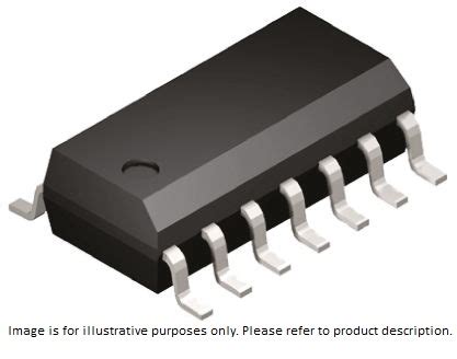
Chip Packaging
Once the IC fabrication process is complete, the individual chips are packaged to protect them from the environment and to facilitate their integration into electronic devices. Some common chip packaging types include:
- Dual Inline Package (DIP)
- Small Outline Integrated Circuit (SOIC)
- Quad Flat Package (QFP)
- Ball Grid Array (BGA)
- Wafer-level Chip Scale Package (WLCSP)

Frequently Asked Questions (FAQ)
-
What is the difference between a semiconductor and an insulator?
A semiconductor has electrical conductivity between that of an insulator and a conductor, and its conductivity can be controlled through various means. An insulator, on the other hand, has very low electrical conductivity and does not allow the flow of electric current. -
Why is silicon the most widely used semiconductor material?
Silicon is abundant, easy to process, and has stable properties, making it an ideal choice for integrated circuit fabrication. Additionally, silicon’s native oxide, silicon dioxide (SiO2), is an excellent insulator, which is crucial for creating insulating layers in ICs. -
What is the purpose of doping in semiconductors?
Doping is the process of introducing impurities into a semiconductor material to modify its electrical properties. By adding elements with more or fewer valence electrons than the semiconductor, the conductivity and the type of charge carriers (electrons or holes) can be controlled. -
How do integrated circuits enable the development of compact and high-performance electronic devices?
Integrated circuits allow for the miniaturization of electronic circuits by fabricating numerous components on a single semiconductor substrate. This miniaturization enables the development of compact, high-performance, and energy-efficient electronic devices, as the components are closer together, reducing signal propagation delays and power consumption. -
What is the difference between an analog IC and a digital IC?
An analog IC processes continuous signals, such as voltage or current levels, and is used in applications like amplifiers, sensors, and power management. A digital IC, on the other hand, processes discrete signals (0s and 1s) and is used in applications like microprocessors, memory devices, and digital logic circuits.
In conclusion, understanding the concepts of semiconductors, wafers, integrated circuits, and chips is essential for anyone interested in electronics. These fundamental components form the backbone of modern electronic devices, enabling the development of compact, high-performance, and energy-efficient systems that have revolutionized our world.


Leave a Reply