Introduction to PCB Soldering Defects
Printed Circuit Boards (PCBs) are essential components in modern electronic devices, providing a platform for mounting and interconnecting electronic components. The quality of solder joints on PCBs directly impacts the reliability and performance of the entire device. Soldering defects can lead to malfunctions, short circuits, and even complete failure of the electronic product. Therefore, identifying and addressing PCB Soldering Defects is crucial for ensuring the quality and longevity of electronic devices.
In this article, we will explore various types of PCB soldering defects, their causes, and methods for prevention and correction. We will also discuss the importance of proper soldering techniques and quality control measures in the PCB manufacturing process.
Types of PCB Soldering Defects
1. Bridging
Bridging, also known as solder bridges, occurs when excess solder forms an unintended connection between two or more adjacent pads or traces on a PCB. This defect can cause short circuits and lead to malfunctions in the electronic device.
Causes of Bridging:
- Excessive solder paste application
- Improper solder paste stencil design
- Incorrect component placement
- Insufficient solder mask between pads
- Incorrect reflow oven temperature profile
Prevention and Correction:
- Optimize solder paste stencil design and aperture sizes
- Ensure proper component placement using automated pick-and-place machines
- Maintain appropriate solder mask clearance between pads
- Adjust reflow oven temperature profile to achieve optimal solder flow
- Use automated optical inspection (AOI) systems to detect bridging defects
- Manually remove excess solder using a soldering iron and solder wick
2. Cold Solder Joints
Cold solder joints occur when the solder fails to melt and flow properly, resulting in a weak and unreliable connection between the component and the PCB pad. These joints appear dull, rough, and may have a cracked or grainy appearance.
Causes of Cold Solder Joints:
- Insufficient heat during the soldering process
- Inadequate flux activity
- Contaminated or oxidized surfaces
- Incorrect solder alloy composition
- Excessive cooling rate after soldering
Prevention and Correction:
- Ensure proper soldering iron temperature and tip condition
- Use high-quality solder alloys with the appropriate melting point
- Apply sufficient flux to promote solder flow and prevent oxidation
- Clean and prepare component leads and PCB pads before soldering
- Control the cooling rate to allow proper solder solidification
- Reheat and resolder the affected joints using the correct technique
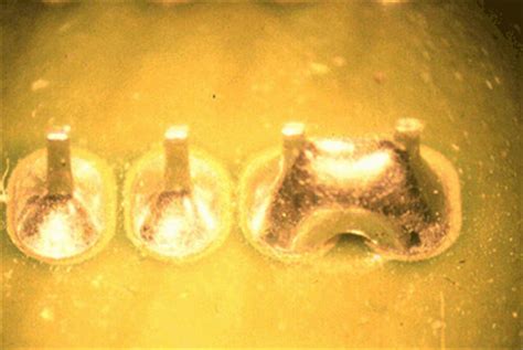
3. Tombstoning
Tombstoning, also known as chipout or drawbridging, is a defect that occurs when a surface-mount component (SMD) stands up on one end, resembling a tombstone. This defect is often caused by uneven heating or an imbalance in solder paste volume between the component pads.
Causes of Tombstoning:
- Uneven heating during the reflow soldering process
- Imbalanced solder paste volume on component pads
- Incorrect component placement or misalignment
- Inadequate or excessive solder paste
- Incorrect reflow oven temperature profile
Prevention and Correction:
- Ensure even heating during the reflow soldering process
- Balance solder paste volume on component pads using proper stencil design
- Use automated pick-and-place machines for accurate component placement
- Optimize solder paste volume and stencil aperture design
- Adjust reflow oven temperature profile to achieve uniform heating
- Manually reposition and resolder the affected components
4. Insufficient Solder
Insufficient solder, also known as dry joints or starved joints, occurs when there is not enough solder to form a proper connection between the component and the PCB pad. These joints appear concave, with visible gaps or voids between the component lead and the pad.
Causes of Insufficient Solder:
- Inadequate solder paste application
- Incorrect solder paste stencil design or aperture size
- Excessive solder paste scooping during stencil printing
- Improper component placement or lead clinching
- Insufficient heat during the soldering process
Prevention and Correction:
- Optimize solder paste stencil design and aperture sizes
- Ensure proper solder paste application using automated stencil printers
- Verify component placement and lead alignment before soldering
- Provide sufficient heat during the soldering process
- Use automated optical inspection (AOI) systems to detect insufficient solder
- Add additional solder using a soldering iron and solder wire
5. Solder Balling
Solder balling is a defect characterized by the formation of small, spherical balls of solder on the PCB surface or component pads. These solder balls can cause short circuits and lead to device malfunction if they come into contact with adjacent components or traces.
Causes of Solder Balling:
- Excessive solder paste application
- Incorrect solder paste composition or particle size
- Improper solder paste stencil design or aperture size
- Inadequate or contaminated flux
- Incorrect reflow oven temperature profile
Prevention and Correction:
- Optimize solder paste stencil design and aperture sizes
- Use solder paste with the appropriate composition and particle size
- Ensure proper flux activity and cleanliness
- Adjust reflow oven temperature profile to minimize solder spattering
- Implement automated optical inspection (AOI) to detect solder balls
- Remove solder balls using a soldering iron, tweezers, or specialized vacuum tools

Importance of Proper Soldering Techniques
Proper soldering techniques are essential for achieving high-quality solder joints and preventing PCB soldering defects. Some key considerations include:
-
Temperature Control: Maintaining the correct soldering iron temperature is crucial for achieving proper solder flow and preventing defects such as cold solder joints or excessive heat damage.
-
Flux Selection: Choosing the appropriate flux type and ensuring its proper application helps remove oxides, promote solder flow, and prevent defects like bridging or insufficient solder.
-
Solder Alloy Selection: Using solder alloys with the appropriate melting point, composition, and particle size ensures compatibility with the PCB materials and helps prevent defects such as solder balling or tombstoning.
-
Soldering Tip Maintenance: Regular cleaning and tinning of soldering iron tips maintain their heat transfer efficiency and prevent contamination, leading to more consistent and reliable solder joints.
-
Operator Training: Providing comprehensive training to soldering operators on proper techniques, defect identification, and correction methods helps ensure consistent quality and reduces the occurrence of PCB soldering defects.

Quality Control Measures in PCB Manufacturing
Implementing effective quality control measures throughout the PCB manufacturing process is essential for minimizing soldering defects and ensuring the overall quality of the final product. Some key quality control measures include:
-
Automated Optical Inspection (AOI): AOI systems use high-resolution cameras and advanced image processing algorithms to detect soldering defects such as bridging, insufficient solder, or tombstoning. These systems provide fast and accurate inspection, enabling early detection and correction of defects.
-
X-Ray Inspection: X-ray inspection systems allow non-destructive examination of solder joints, particularly for hidden or obscured connections such as ball grid arrays (BGAs) or quad flat no-lead (QFN) packages. This technology helps identify defects like voids, shorts, or misalignments that may not be visible through optical inspection.
-
In-Circuit Testing (ICT): ICT involves using specialized test fixtures and probes to verify the electrical connectivity and functionality of individual components and circuits on a PCB. This testing method helps identify soldering defects that may cause open or short circuits, as well as component failures.
-
Functional Testing: Functional testing involves subjecting the assembLED PCB to its intended operating conditions and verifying its performance against specified requirements. This testing stage helps identify any soldering defects that may impact the overall functionality or reliability of the electronic device.
-
Statistical Process Control (SPC): Implementing SPC methods involves collecting and analyzing process data to monitor the stability and capability of the soldering process. By tracking key process parameters such as temperature, time, and solder paste volume, manufacturers can identify trends and make data-driven decisions to optimize the process and reduce the occurrence of soldering defects.

FAQ
-
Q: What are the most common PCB soldering defects?
A: The most common PCB soldering defects include bridging, cold solder joints, tombstoning, insufficient solder, and solder balling. Each defect has its own characteristics, causes, and impacts on the reliability and functionality of the electronic device. -
Q: How can PCB soldering defects be prevented?
A: PCB soldering defects can be prevented by implementing proper soldering techniques, such as maintaining the correct soldering iron temperature, using appropriate flux and solder alloys, ensuring proper solder paste application, and providing comprehensive training to soldering operators. Additionally, effective quality control measures like automated optical inspection (AOI) and statistical process control (SPC) help identify and correct defects early in the manufacturing process. -
Q: What are the consequences of PCB soldering defects?
A: PCB soldering defects can lead to various consequences, including short circuits, open connections, intermittent failures, and reduced reliability of the electronic device. These defects can cause malfunctions, performance degradation, and even complete failure of the product, resulting in costly rework, repairs, or customer returns. -
Q: How can PCB soldering defects be corrected?
A: The correction method for PCB soldering defects depends on the specific type of defect. Some common correction techniques include manual soldering using a soldering iron and solder wick to remove excess solder or add missing solder, repositioning misaligned components, and using specialized tools like tweezers or vacuum devices to remove solder balls. In some cases, the affected components may need to be replaced entirely. -
Q: What role does quality control play in minimizing PCB soldering defects?
A: Quality control measures play a crucial role in minimizing PCB soldering defects by enabling early detection, analysis, and correction of defects throughout the manufacturing process. Automated Inspection systems, such as AOI and X-ray inspection, provide fast and accurate defect detection, while testing methods like ICT and functional testing help verify the electrical and functional performance of the assembled PCB. Implementing statistical process control (SPC) allows manufacturers to monitor and optimize the soldering process based on data-driven insights, reducing the occurrence of defects and improving overall product quality.
Conclusion
PCB soldering defects pose significant challenges to the reliability and performance of electronic devices. Understanding the various types of defects, their causes, and methods for prevention and correction is essential for ensuring the quality and longevity of PCBs. By implementing proper soldering techniques, comprehensive operator training, and effective quality control measures, manufacturers can minimize the occurrence of soldering defects and produce high-quality, reliable electronic products.
As the electronics industry continues to evolve, with increasing miniaturization and complexity of components, addressing PCB soldering defects will remain a critical aspect of the manufacturing process. Continuous improvement in soldering technologies, materials, and processes, along with the adoption of advanced inspection and testing methods, will be key to meeting the ever-growing demands for quality and reliability in electronic devices.
[Word count: 1852 words]


Leave a Reply