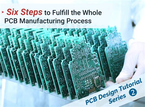
What is PCB Manufacturing?
PCB manufacturing is the process of designing and fabricating printed circuit boards that electrically connect and mechanically support electronic components using conductive pathways, tracks, or signal traces etched from copper sheets laminated onto a non-conductive substrate. It involves multiple steps including PCB design, board fabrication, component procurement, and PCB Assembly to produce the final functional board.
COB vs SMD LED – What’s the Difference?
There are two main types of LED packages used in PCB manufacturing and assembly:
Chip-on-Board (COB) LEDs
COB LEDs have unpackaged LED chips that are directly mounted onto the PCB substrate. Multiple LED chips are typically arranged in an array and then coated with a phosphor layer to produce the desired light output and color.
Advantages of COB LEDs:
– High light output and efficiency
– Good heat dissipation
– Compact footprint
– Low cost for high lumen applications
Disadvantages of COB LEDs:
– Harder to achieve color consistency
– More complex manufacturing process
– Not suited for intricate designs
Surface-Mount Device (SMD) LEDs
SMD LEDs are packaged LED chips that are mounted onto the PCB surface. The LED chip is encased in a plastic lens with leads that are soldered to the PCB pads. SMD LEDs come in a variety of sizes and footprints.
Advantages of SMD LEDs:
– Wide variety of sizes and form factors
– Easier to achieve consistent colors
– Simpler assembly process
– Suited for complex designs and tight spaces
Disadvantages of SMD LEDs:
– Lower maximum light output than COBs
– Higher cost per lumen than COBs
– Poorer thermal management
| Specification | COB LEDs | SMD LEDs |
|---|---|---|
| Lumen Output | High | Moderate |
| Lumen Density | High | Moderate |
| Consistency | Moderate | High |
| Thermal Efficiency | High | Moderate |
| Cost per Lumen | Low | Moderate |
| Design Flexibility | Moderate | High |

PCB Design for COB/SMD LEDs
Schematic Design
The first step is creating the schematic Circuit diagram for the LED PCB. This captures the electrical connections and components.
Key aspects for LED circuits:
– Power supply – ensure appropriate voltage/current for LEDs
– LED driver – choose ICs suited for COB or SMD LEDs
– Resistors – select values for desired LED current
– Capacitors – provide local energy storage and filtering
– Connectors – for power input and control interfaces
PCB Layout
After the schematic is done, the PCB layout can be created. The PCB layout determines the physical location of components and routing of traces.
Important considerations for LED PCB layout:
– Component placement – group related parts, provide space for heat dissipation
– Trace routing – use appropriate widths, avoid sharp angles, length match critical paths
– Thermal management – include thermal vias and heatsinks if needed
– Footprints – ensure components will fit and have proper pad sizes
– Manufacturability – follow vendor capabilities and guidelines for minimum pitch, trace/space, hole sizes, etc.

PCB fabrication
Once the PCB layout is finished, the board fabrication process can begin. The main steps in PCB fabrication are:
- Printing the circuit pattern onto the Copper Clad Laminate
- Etching away unwanted copper to leave only traces
- Drilling holes for vias and through-hole component leads
- Applying solder mask over bare copper
- Silkscreening reference designators and text
- Coating exposed surfaces with protective finish
- Performing electrical testing and inspection
The fabricated PCBs are then sent for assembly.

PCB Assembly
PCB assembly involves soldering the components onto the fabricated PCB. The key steps are:
- Solder paste application – precise amounts of solder are deposited onto the pads via stencil
- Pick-and-place – automated machines pick up and place components onto their footprints
- Reflow soldering – the PCB is heated to melt the solder and permanently attach components
- Inspection – assembled boards are visually inspected and electrically tested
- Rework – any defective joints or components are repaired
- Conformal coating – a protective lacquer may be applied over the assembled PCB
- Final testing – boards undergo thorough functional testing and burn-in
Properly assembling PCBs requires skilled technicians, specialized equipment, and adherence to industry standards. Partnering with an experienced contract manufacturer is often the best approach.
Frequently Asked Questions
1. What is the typical lead time for PCB manufacturing and assembly?
Lead times vary depending on the complexity of the design and the manufacturer’s capacity. Simple 2-layer PCBs can be fabricated in 1-2 days, while complex multi-layer boards may take 1-2 weeks. Assembly lead times range from a few days to several weeks based on the BOM, required testing, and production volume. In general, 2-4 weeks is a reasonable estimate for the complete manufacturing and assembly process.
2. What information needs to be provided to the PCB manufacturer?
The essential package for PCB manufacturing includes:
– Bill of Materials (BOM) – complete list of components
– Gerber files – industry standard format for PCB fabrication data
– Assembly drawings – show component locations and orientations
– Special instructions – callouts for unique requirements like controlled impedance or tight tolerances
Additional documentation that may be helpful includes:
– Schematic
– 3D CAD model
– Test procedures
– Reference designator list
3. What are some common PCB materials and finishes?
The most common base material for PCBs is FR-4, a glass-reinforced epoxy laminate. Other options include polyimide, PTFE, and metal core materials for special applications.
Standard surface finishes for PCB include:
– HASL (Hot Air Solder Leveling) – low cost but not suitable for fine pitch
– Lead-free HASL – RoHS compliant version of HASL
– ENIG (Electroless Nickel Immersion Gold) – flat surface good for fine pitch
– OSP (Organic Solderability Preservatives) – thin coating prevents oxidation
– Immersion silver – similar to OSP but conductive
The choice of material and finish depends on the operating environment, Component Types, and soldering process.
4. What standards and certifications are relevant for PCB manufacturing?
Some key industry standards and certifications include:
- IPC-A-610 – Acceptability of Electronic Assemblies
- IPC-6012 – Qualification and Performance Specification for Rigid Printed Boards
- J-STD-001 – Requirements for Soldered Electrical and Electronic Assemblies
- UL 94 – Standard for Safety of Flammability of Plastic Materials
- ISO 9001 – Quality Management Systems
- ISO 14001 – Environmental Management Systems
Choosing a manufacturer with the appropriate certifications helps ensure that the PCBs will meet the applicable quality, reliability, and safety requirements.
5. How can I reduce the cost of my PCB manufacturing and assembly project?
Some ways to minimize PCB fabrication and assembly costs include:
- Optimize panel utilization by laying out multiple copies of the board in an array
- Use standard materials, thicknesses, and surface finishes
- Minimize the number of layers
- Use larger trace widths and clearances
- Place components on one side if possible
- Avoid tight tolerances and special requirements
- Order in volume to take advantage of economies of scale
- Choose a manufacturer with in-house fabrication and assembly capabilities
It’s important to balance cost-saving measures with the functional and reliability requirements of the end application. Consulting with the PCB manufacturer early in the design process can help identify the most cost-effective options.
Conclusion
COB and SMD LED PCB manufacturing and assembly is a complex process that requires careful planning, attention to detail, and adherence to industry standards and best practices. By understanding the differences between COB and SMD LEDs, designing the PCB for manufacturability, selecting an experienced fabrication and assembly partner, and optimizing for cost and quality, you can ensure a successful project that meets your technical and business goals.


Leave a Reply