What is BGA?
BGA, or Ball Grid Array, is a type of surface-mount packaging used for integrated circuits (ICs) that utilizes a grid of solder balls as the connection points between the package and the printed circuit board (PCB). This packaging technology has gained significant popularity in recent years due to its numerous advantages over traditional packaging methods, such as quad flat packages (QFP) and pin grid arrays (PGA).
BGA Packages offer several benefits, including:
- Higher pin count density
- Improved electrical and thermal performance
- Better signal integrity
- Reduced package size
- Enhanced reliability
Types of BGA Packages
There are several types of BGA packages, each designed to cater to specific applications and requirements. Some of the most common BGA package types include:
| Package Type | Description |
|---|---|
| Plastic BGA (PBGA) | A cost-effective solution for consumer electronics and low-power applications |
| Ceramic BGA (CBGA) | Offers superior thermal and electrical performance for high-reliability applications |
| Tape BGA (TBGA) | Uses a thin, flexible tape substrate for reduced package thickness and improved flexibility |
| Flip Chip BGA (FCBGA) | Utilizes a flip chip die attachment method for enhanced performance and reduced package size |
BGA Package Structure
A typical BGA package consists of several key components:
- Die: The integrated circuit or chip that performs the desired functions
- Substrate: The base material that provides mechanical support and electrical connectivity between the die and the solder balls
- Wire bonds or flip chip bumps: The electrical connections between the die and the substrate
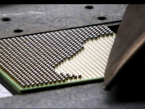
- Solder balls: The conductive balls that form the connection points between the package and the PCB
- Encapsulant or lid: Protects the die and wire bonds from environmental factors
BGA Substrate Materials
BGA substrates can be made from various materials, each with its own advantages and disadvantages. The most common substrate materials include:
| Material | Advantages | Disadvantages |
|---|---|---|
| Bismaleimide Triazine (BT) | Good electrical and thermal properties, cost-effective | Limited high-frequency performance |
| Polyimide | Excellent thermal stability and flexibility | Higher cost compared to BT |
| Ceramic | Superior thermal and electrical performance, high reliability | Expensive, brittle, and difficult to process |

BGA Assembly Process
The BGA assembly process involves several critical steps to ensure a reliable and high-quality final product. The main stages of BGA assembly include:
- Solder paste printing: Applying solder paste to the PCB pads using a stencil
- BGA package placement: Positioning the BGA package on the PCB using a pick-and-place machine
- Reflow soldering: Heating the assembly to melt the solder paste and form a strong bond between the package and the PCB
- Inspection and testing: Verifying the quality of the solder joints and the functionality of the assembled device
Challenges in BGA Assembly
While BGA technology offers numerous benefits, it also presents some challenges during the assembly process. Some of the most common challenges include:
- Solder joint reliability: Ensuring consistent and reliable solder joint formation across the entire BGA package
- Thermal management: Dissipating heat effectively to prevent thermal stress and package failure
- Warpage control: Minimizing substrate and PCB Warpage during reflow soldering to maintain solder joint integrity
- Rework and repair: Difficulty in removing and replacing BGA packages without damaging the PCB or neighboring components

BGA Design Considerations
To ensure a successful BGA assembly and reliable performance, several design considerations must be taken into account. Some key factors to consider when designing BGA-based PCBs include:
- Pad size and pitch: Selecting appropriate pad sizes and pitches based on the BGA package dimensions and PCB manufacturing capabilities
- Solder mask design: Ensuring proper solder mask openings and clearances to prevent solder bridging and short circuits
- Thermal management: Incorporating thermal vias and heat spreaders to dissipate heat effectively and prevent thermal stress
- Signal integrity: Optimizing PCB Layout and routing to minimize signal distortion and crosstalk, especially for high-speed applications
BGA Routing Strategies
Proper PCB Routing is crucial for maintaining signal integrity and minimizing electromagnetic interference (EMI) in BGA-based designs. Some common BGA routing strategies include:
| Routing Strategy | Description |
|---|---|
| Fan-out | Routing traces from the BGA pads to the outer layers of the PCB |
| Dog-bone | Using short traces to connect BGA pads to vias, which then connect to the desired layers |
| Via-in-pad | Placing vias directly on the BGA pads to route signals to inner layers |
| Microvia | Utilizing small, laser-drilled vias for high-density BGA routing |

BGA Testing and Inspection
To ensure the quality and reliability of BGA assemblies, various testing and inspection methods are employed. Some common techniques include:
- X-ray inspection: Using X-ray imaging to verify solder joint quality and detect any voids or bridging
- Automated optical inspection (AOI): Utilizing machine vision to inspect solder joints and component placement
- Boundary scan testing: Employing built-in test circuitry to verify the functionality of BGA-based devices
- Thermal cycling: Subjecting the assembly to temperature fluctuations to assess its reliability under varying environmental conditions
BGA Failure Modes and Analysis
Despite the numerous advantages of BGA technology, failures can still occur due to various factors. Some common BGA failure modes include:
| Failure Mode | Description |
|---|---|
| Solder joint fatigue | Cracking or fracturing of solder joints due to thermal stress or mechanical strain |
| Solder joint voids | Air pockets within the solder joints that can reduce mechanical strength and thermal conductivity |
| Warpage-induced failures | Solder joint disconnections or fractures caused by excessive substrate or PCB warpage |
| Electromigration | The gradual displacement of metal ions in the solder joints due to high current densities, leading to voids and eventual failure |
To analyze and diagnose BGA failures, techniques such as scanning electron microscopy (SEM), energy-dispersive X-ray spectroscopy (EDX), and cross-sectioning are often employed.
Future Trends in BGA Technology
As electronic devices continue to become more compact and sophisticated, BGA technology is evolving to meet the ever-increasing demands for performance, reliability, and miniaturization. Some of the future trends in BGA technology include:
- Finer pitch and smaller solder balls: Enabling higher pin count densities and more compact package sizes
- Advanced substrate materials: Developing new substrate materials with improved electrical, thermal, and mechanical properties
- 3D packaging: Stacking multiple BGA packages vertically to create high-density, three-dimensional assemblies
- Embedded components: Integrating passive components, such as capacitors and resistors, within the BGA substrate to save space and improve performance
Conclusion
BGA technology has revolutionized the electronics industry by offering numerous advantages over traditional packaging methods. Its high pin count density, improved electrical and thermal performance, and compact size have made it an essential choice for a wide range of applications, from consumer electronics to high-reliability systems.
However, designing and assembling BGA-based PCBs requires careful consideration of various factors, such as substrate material selection, pad size and pitch, thermal management, and signal integrity. Proper testing and inspection techniques are also crucial for ensuring the quality and reliability of BGA assemblies.
As electronic devices continue to evolve, BGA technology will likely keep pace with advancements in substrate materials, packaging techniques, and miniaturization. By staying informed about the latest trends and best practices in BGA technology, engineers and manufacturers can create innovative, high-performance products that meet the demands of the ever-changing electronics landscape.
Frequently Asked Questions (FAQ)
- What is the main difference between BGA and QFP packaging?
-
BGA packages use a grid of solder balls as connection points, while QFP packages utilize peripheral leads. BGA packages offer higher pin count density and better electrical and thermal performance compared to QFP packages.
-
Can BGA packages be reworked or repaired?
-
Reworking or repairing BGA packages can be challenging due to the difficulty in accessing and removing the package without damaging the PCB or neighboring components. Specialized equipment and techniques, such as hot air rework stations and reballing, are often required for successful BGA Rework.
-
What is the purpose of thermal vias in BGA-based PCB designs?
-
Thermal vias are used to dissipate heat from the BGA package to the other layers of the PCB. By providing a low-resistance path for heat transfer, thermal vias help prevent thermal stress and improve the overall reliability of the assembly.
-
How does X-ray inspection help in evaluating BGA solder joint quality?
-
X-ray inspection allows for non-destructive visualization of the solder joints beneath the BGA package. This technique can reveal voids, bridging, and other defects that may not be visible through optical inspection methods, enabling engineers to assess the quality and reliability of the solder joints.
-
What are the advantages of using flip chip BGA packages?
- Flip chip BGA packages offer several advantages, including reduced package size, improved electrical performance, and better thermal management. By eliminating the need for wire bonds, flip chip BGA packages minimize signal path lengths and parasitic inductances, resulting in enhanced signal integrity and faster signal propagation.


Leave a Reply