Introduction to PCB Routing
PCB routing is the process of creating electrical connections between components on a printed circuit board (PCB). It is a crucial step in the PCB design process, as it directly affects the functionality, reliability, and manufacturability of the final product. For beginners, PCB routing can be a daunting task, but with the right knowledge and techniques, it can be mastered.
In this article, we will discuss various PCB routing tips and best practices that can help beginners create high-quality PCB designs. We will cover topics such as understanding the PCB Stack-Up, selecting the appropriate trace width, minimizing crosstalk, and optimizing signal integrity.
Understanding the PCB Stack-up
What is a PCB Stack-up?
A PCB stack-up refers to the arrangement of layers in a PCB. It defines the number of layers, their order, and the materials used for each layer. The stack-up plays a significant role in the overall performance of the PCB, as it affects signal integrity, impedance, and electromagnetic compatibility (EMC).
Common PCB Stack-up Configurations
There are several common PCB stack-up configurations, each with its own advantages and disadvantages. The following table summarizes some of the most common stack-up configurations:
| Stack-up Configuration | Layers | Advantages | Disadvantages |
|---|---|---|---|
| Single-layer | 1 | Low cost, simple design | Limited routing options, poor EMC performance |
| Double-layer | 2 | Improved routing options, better EMC performance | Higher cost than single-layer |
| Four-layer | 4 | Excellent routing options, good EMC performance, suitable for high-speed designs | Higher cost than double-layer |
| Six-layer | 6 | Increased routing density, improved signal integrity, suitable for complex designs | Higher cost than four-layer, more complex design process |
When selecting a stack-up configuration, consider factors such as the complexity of your design, the required performance, and the budget constraints.

Selecting the Appropriate Trace Width
Factors Affecting Trace Width Selection
The trace width is the width of the copper tracks on the PCB. Selecting the appropriate trace width is crucial for ensuring proper current carrying capacity, minimizing resistance, and maintaining signal integrity. The following factors should be considered when selecting the trace width:
- Current carrying capacity: The trace width must be sufficient to handle the maximum current flowing through the trace without causing excessive heating or voltage drop.
- Resistance: Narrower traces have higher resistance, which can lead to voltage drop and signal degradation.
- Manufacturing constraints: The minimum trace width is limited by the manufacturing capabilities of the PCB fabricator.
Calculating the Appropriate Trace Width
To calculate the appropriate trace width, you can use online calculators or refer to the IPC-2221 standard, which provides guidelines for trace width based on the current carrying capacity and temperature rise. The following table shows some common trace width values for different current ratings:
| Current Rating (A) | Trace Width (mm) |
|---|---|
| 0.5 | 0.2 |
| 1.0 | 0.3 |
| 2.0 | 0.5 |
| 3.0 | 0.8 |
Keep in mind that these values are just guidelines, and the actual trace width may vary depending on the specific requirements of your design.

Minimizing Crosstalk
What is Crosstalk?
Crosstalk is the unwanted coupling of signals between adjacent traces on a PCB. It occurs when the electromagnetic field generated by one signal interferes with another signal, causing signal distortion and degradation. Crosstalk is a common issue in high-speed PCB designs and can lead to signal integrity problems if not properly addressed.
Techniques for Minimizing Crosstalk
There are several techniques that can be used to minimize crosstalk in PCB designs:
- Increase trace spacing: Increasing the spacing between adjacent traces reduces the coupling between them, thus minimizing crosstalk.
- Use guard traces: Placing grounded guard traces between sensitive signals can help shield them from crosstalk.
- Route signals on different layers: Routing sensitive signals on different layers of the PCB can help isolate them from each other, reducing crosstalk.
- Use differential signaling: Differential signaling techniques, such as LVDS (Low-Voltage Differential Signaling), can help cancel out the effects of crosstalk by transmitting signals as a pair of complementary signals.

Optimizing Signal Integrity
What is Signal Integrity?
Signal integrity refers to the ability of a signal to maintain its intended characteristics as it propagates through the PCB. Factors such as impedance mismatch, reflections, and crosstalk can degrade signal integrity, leading to signal distortion, timing errors, and other issues.
Techniques for Optimizing Signal Integrity
To optimize signal integrity in PCB designs, consider the following techniques:
- Impedance matching: Ensure that the impedance of the trace matches the impedance of the source and load to minimize reflections and signal distortion.
- Termination: Use appropriate termination techniques, such as series termination or parallel termination, to minimize reflections and improve signal quality.
- Length matching: Match the length of traces carrying related signals to minimize timing skew and ensure proper signal synchronization.
- Avoid sharp corners: Use smooth corners and avoid sharp bends in traces to minimize reflections and signal distortion.
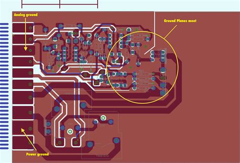
- Use ground planes: Incorporate ground planes in the PCB stack-up to provide a low-impedance return path for signals and reduce EMI.
Frequently Asked Questions (FAQ)
1. What is the difference between a trace and a via in PCB routing?
A trace is a copper track on the surface of the PCB that connects components, while a via is a hole drilled through the PCB that allows signals to pass from one layer to another.
2. How do I choose the right PCB stack-up for my design?
When choosing a PCB stack-up, consider factors such as the complexity of your design, the required performance, and the budget constraints. Consult with your PCB fabricator to determine the best stack-up configuration for your specific needs.
3. What is the minimum trace width I can use in my PCB design?
The minimum trace width depends on the manufacturing capabilities of your PCB fabricator. Typically, the minimum trace width ranges from 0.1 mm to 0.2 mm, but it can vary depending on the fabricator and the specific requirements of your design.
4. How can I minimize the impact of crosstalk in my PCB design?
To minimize crosstalk, you can increase trace spacing, use guard traces, route signals on different layers, and employ differential signaling techniques such as LVDS.
5. What is the importance of impedance matching in PCB routing?
Impedance matching is crucial for maintaining signal integrity in PCB designs. By ensuring that the impedance of the trace matches the impedance of the source and load, you can minimize reflections and signal distortion, resulting in a more reliable and robust PCB design.
Conclusion
PCB routing is a critical aspect of PCB design that requires careful consideration and attention to detail. By understanding the PCB stack-up, selecting the appropriate trace width, minimizing crosstalk, and optimizing signal integrity, beginners can create high-quality PCB designs that meet their specific requirements.
Remember to consult with your PCB fabricator, follow industry standards and guidelines, and continuously refine your skills through practice and learning. With dedication and persistence, you can master the art of PCB routing and create PCBs that are reliable, efficient, and meet the demands of today’s electronic devices.


Leave a Reply