Introduction
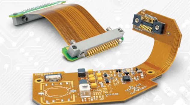
Flex PCBs (flexible printed circuit boards) are a critical technology that enables flexible circuits and connections in modern electronic devices. As products continue getting smaller and more portable, flex PCBs have become indispensable for smart wearables, folded displays, and devices with moving parts.
However, flex PCB design brings unique challenges compared to rigid PCBs. The flexible layers can be tricky to configure and route traces through while maintaining performance and reliability. This is where Altium’s layer stack manager comes into play – providing powerful tools to optimize complex flex stackups.
In this guide, we’ll explore how Altium’s layer stack manager enables easier flex PCB design. We’ll cover key features like defining flex stackups, managing rules and constraints, and visualizing flex layer deformations. Read on to learn how Altium can help you conquer the intricacies of flex PCBs.
Overview of Flexible PCBs
Let’s first briefly go over what makes flex PCBs unique:
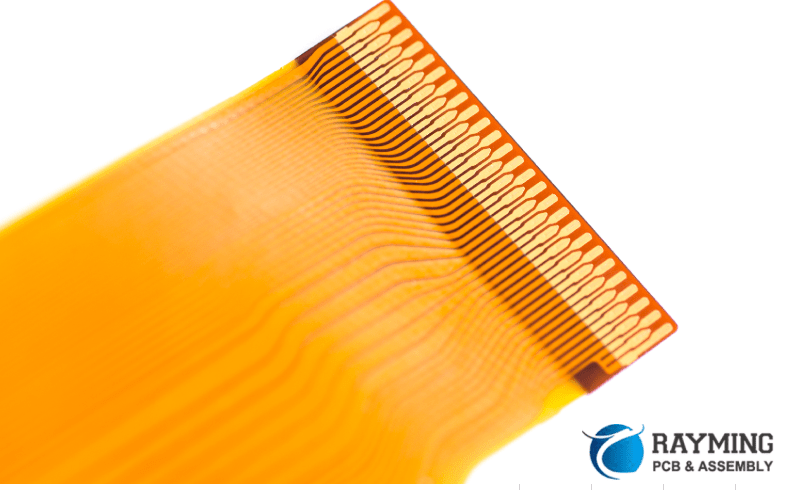
- Flexible substrate materials – The base material is a thin, flexible polymer like polyimide instead of traditional rigid FR4. This allows the PCB to bend and flex without damage.
- Flexible layers – Conductive traces are laid out on the flexible substrate to interconnect components. Special flex-capable layers are used instead of standard copper.
- Bend zones – Areas of the PCB that are designed to repeatedly bend during use. Traces here require careful layout.
- Rigid sections – Regions that remain rigid for mounting components and connectors. Stiffeners are often added for support.
- Dynamic flexing – Flex PCBs are designed to move and bend in application, requiring extensive modeling and analysis.
With these traits in mind, let’s look at how Altium’s tools simplify the process of designing and laying out flex PCBs.
Creating Flex Layer Stacks
The foundation of any PCB design is the layer stack – the sequence of conductive copper and insulating dielectric layers. Altium’s layer stack manager provides an intuitive way to configure flex layer stacks with different materials and properties.
To demonstrate, let’s walk through setting up a simple 4-layer flex stack:
- Open the Layer Stack Manager and choose the Flex Stackup Wizard. This will guide you through building the stack step-by-step.
- Enter a name like “4LayerFlex”. Choose number of conductive layers (4) and dielectric layers (3).
- Select flexible substrate materials. For example, polyimide for dielectrics and rolled annealed copper for conductors.
- Arrange core, prepreg, and copper layers. The wizard ensures proper layer ordering.
- Enter additional details like layer thicknesses and copper weights. Define bend zones if needed.
- Review summary of the finished stackup. The manager will visualize the complete layer structure.
With these steps, you’ve configured the critical flex stackup for your design. The manager handles all the intricacies of arranging materials and layers. This takes the guesswork out of defining complex flex constructions.
Managing Layer Constraints
Altium includes powerful tools for defining and visualizing constraints across flex stackups. This is key to ensuring reliable performance under bending and flexing conditions.
Some of the essential flex layer constraints include:
- Bend radius – The minimum bend radius that regions of the PCB can handle without damage.
- Flexibility – Ability of a material to bend, quantified by stiffness.
- Stretchability – How much a material can elongate/compress during bending.
- Neutral axis – The layer with no expansion/compression when bent (usually midpoint).
The Layer Stack Manager lets you enter these kinds of constraints for each layer. It then uses this data to provide visual overlays showing safe bend limits, neutral axis, and more. This helps guide layout and highlight potential issues from over-bending.
You can also define guidelines like trace widths, spacing, and routing layers based on flex characteristics. The design rules system will use these constraints to automatically validate your PCB as you route traces. This helps catch errors so you can keep flex layers within safe limits.
Modeling the Flexed State
One of the biggest advantages of Altium’s layer stack tools is the ability to visually model the flexed state. This provides an invaluable reference as you layout and route the flex layers.
The key process is:
- Define rigid-flex regions and bend axes based on the intended application mechanics.
- Enter realistic bend radius values for each region.
- Use tools like the Flex Bending Gauges to model the PCB in its flexed/bent orientation.
- The layer stack manager will calculate deformations and display each layer in its bent shape.
Having this “bent mode” preview enables you to design with the end state in mind. You can arrange components and route traces optimized for how the layers will actually look when flexed. This helps minimize the risk of failure under real mechanical stresses.
The rigid-flex modeling tools take the guesswork out of anticipating how your PCB will behave when bent in the application. It’s a powerful advantage for ensuring reliability.
Final Words
Altium’s layer stack manager and flex modeling features provide key advantages for demanding flex PCB designs. The intuitive stackup configuration tools allow you to arrange advanced flex constructions with ease. Constraint management helps maintain performance and reliability by defining and visualizing flex limits. And the unique flexed mode modeling provides invaluable insight for laying out traces optimized for the real bent state.
With these capabilities, designers can tackle complex flex PCBs with much greater confidence. The ability to virtually prototype flex stackups and analyze the impact of bending helps resolve problems early, before reaching costly prototyping stages. If your designs need the advantages of flex PCBs, be sure to explore how Altium’s solutions can smooth the process. The layer stack tools are advanced yet accessible, allowing focus on the design rather than fighting with software.
Frequently Asked Questions
What are the key benefits of Altium’s layer stack manager for flex PCBs?
Some of the major benefits include:
- Intuitive flex stackup configuration with pre-defined materials and constraint rules
- Flexible rigid-flex modeling tools to define bend areas and preview deformations
- Visualization overlays for clearly seeing safe bend radii, neutral axis, and more
- Ability to define and check design rules specific to flex layers
- Smoother constraint-driven routing for complex flex layer layout
How are rigid sections of a flex PCB handled in Altium?
Altium allows you to define rigid sections within the layer stackup. These areas can have different layer constructions, with additional stiffening dielectrics and thicker copper if needed. Altium will ensure correct layer ordering and transitions between rigid-flex regions.
What type of analysis features does Altium provide for flex PCBs?
In addition to the layer stack modeling, Altium also includes analysis tools like finite-element thermal simulation. This allows studying heat dissipation under flexing conditions. Signal integrity analysis can also simulate how signals perform across bends. These advanced engines provide valuable insight during flex PCB design.
How do you create bend areas and control trace routing in Altium?
Altium includes both interactive and rules-based tools for managing bend areas:
- Flex Bending Gauges let you visually define bends and interactively route traces.
- Bend constraints defined in the layer stack govern trace widths, spacing, etc.
- Tuned design rules can restrict routing layers and enforce constraints in bend areas.
What file formats does Altium support for importing/exporting flex stackups?
Altium supports widely-used standards like ODB++, IPC-2581, and STEP for passing flex stackup information between tools. The data includes all the materials, constraints, and modeled deformation data. This enables collaborative flex design workflows.


Leave a Reply