What is a Blind Via PCB?
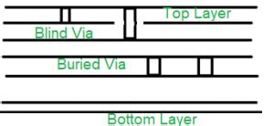
A blind via PCB, also known as a Buried Via PCB, is a type of printed circuit board (PCB) that has vias that are not visible on the surface of the board. These vias are used to connect different layers of the PCB without being exposed on the top or bottom surfaces.
Blind vias are created by drilling a hole that starts at an outer layer and ends at an inner layer, rather than going all the way through the board like a traditional through-hole via. This allows for more compact designs and improved signal integrity.
Advantages of Using Blind Via PCBs
There are several advantages to using blind via PCBs:
-
Increased Density: Blind vias allow for more components and traces to be placed on a smaller board size, which can lead to higher density designs.
-
Improved Signal Integrity: By not going all the way through the board, blind vias can reduce the amount of electromagnetic interference (EMI) and signal reflections that can occur with through-hole vias.
-
Reduced Cost: In some cases, using blind vias can reduce the cost of manufacturing a PCB by allowing for smaller board sizes and fewer layers.
-
Better Thermal Management: Blind vias can be used to transfer heat away from components more efficiently than through-hole vias.

Disadvantages of Using Blind Via PCBs
While there are many advantages to using blind via PCBs, there are also some disadvantages to consider:
-
Increased Manufacturing Complexity: Creating blind vias requires specialized equipment and processes, which can increase the complexity and cost of manufacturing.
-
Limited Layer Access: Blind vias can only connect to inner layers that are adjacent to the outer layer where the via starts. This can limit the design options available.
-
Reduced Reliability: Blind vias can be more prone to failure than through-hole vias, particularly if they are not properly designed or manufactured.

Types of Blind Vias
There are several different types of blind vias that can be used in PCB design:
| Type | Description |
|---|---|
| Blind Via | Connects an outer layer to an inner layer |
| Buried Via | Connects two inner layers without being exposed on the surface |
| Skip Via | Connects an outer layer to an inner layer, skipping one or more layers in between |
| Staggered Via | Two or more blind vias that are staggered to connect multiple layers |

Design Considerations for Blind Via PCBs
When designing a PCB with blind vias, there are several key factors to consider:
-
Via Size: The size of the blind via will depend on the thickness of the PCB and the number of layers being connected. Smaller vias can allow for higher density designs but may be more difficult to manufacture.
-
Via Placement: Blind vias should be placed in areas where they will not interfere with other components or traces on the board. They should also be placed to minimize the length of the signal path.
-
Via Spacing: The spacing between blind vias should be carefully considered to ensure proper signal integrity and manufacturability.
-
Layer Stack-Up: The layer stack-up of the PCB should be designed to accommodate the blind vias and ensure proper connectivity between layers.
Manufacturing Process for Blind Via PCBs
The manufacturing process for blind via PCBs involves several specialized steps:
-
Drilling: The first step is to drill the blind vias using a laser or mechanical drill. The depth of the via is carefully controlled to ensure it reaches the desired inner layer.
-
Plating: After drilling, the vias are plated with a conductive material, typically copper, to create an electrical connection between the layers.
-
Filling: In some cases, the blind vias may be filled with a non-conductive material to improve the structural integrity of the board and prevent contamination.
-
Lamination: The layers of the PCB are then laminated together under high pressure and temperature to create a solid board.
-
Etching: The copper traces on the outer layers are etched away to create the desired circuit pattern.
-
Solder Mask: A solder mask is applied to the outer layers to protect the copper traces and prevent short circuits.
-
Surface Finish: Finally, a surface finish, such as ENIG or HASL, is applied to the exposed copper to prevent oxidation and improve solderability.
Testing and Inspection of Blind Via PCBs
After manufacturing, blind via PCBs must undergo thorough testing and inspection to ensure they meet the required specifications and performance criteria. Some common tests include:
-
Continuity Test: This test verifies that all the connections on the board are correct and there are no open circuits.
-
Isolation Test: This test checks for any short circuits or leakage between adjacent traces or components.
-
Microsection Analysis: This involves cutting a small section of the board and examining it under a microscope to verify the quality of the blind vias and plating.
-
Thermal Cycling: The board may be subjected to repeated heating and cooling cycles to ensure it can withstand the expected operating conditions.
-
X-Ray Inspection: X-ray imaging can be used to inspect the internal structure of the board and verify the placement and quality of the blind vias.
Frequently Asked Questions (FAQ)
-
What is the difference between a blind via and a buried via?
A blind via connects an outer layer to an inner layer, while a buried via connects two inner layers without being exposed on the surface. -
Can blind vias be used on any type of PCB?
Blind vias can be used on most types of PCBs, including rigid, flexible, and rigid-flex boards. However, the specific design and manufacturing requirements may vary depending on the type of board. -
How small can a blind via be?
The minimum size of a blind via depends on the thickness of the PCB and the capabilities of the manufacturing process. Typically, blind vias can be as small as 0.1mm in diameter, although smaller sizes may be possible with advanced manufacturing techniques. -
Are blind vias more expensive than through-hole vias?
In general, blind vias are more expensive to manufacture than through-hole vias due to the specialized equipment and processes required. However, the overall cost of the PCB may be lower if using blind vias allows for a smaller board size or fewer layers. -
How can I ensure the reliability of blind vias in my PCB design?
To ensure the reliability of blind vias, it is important to follow best practices for PCB design, including properly sizing and spacing the vias, selecting appropriate materials and finishes, and thoroughly testing and inspecting the manufactured boards. Working with an experienced PCB manufacturer can also help ensure the quality and reliability of the final product.
Conclusion
Blind via PCBs offer many advantages over traditional through-hole designs, including increased density, improved signal integrity, and reduced cost. However, they also require specialized manufacturing processes and careful design considerations to ensure reliability and performance.
By understanding the key elements of blind via PCBs, including the types of vias, design considerations, manufacturing processes, and testing requirements, designers can create high-quality, reliable PCBs that meet the demands of modern electronic devices.
As technology continues to advance, the use of blind via PCBs is likely to become even more widespread, enabling smaller, faster, and more complex electronic devices. By staying up-to-date with the latest developments in PCB design and manufacturing, designers can ensure they are well-positioned to take advantage of these new opportunities and create innovative products that meet the needs of their customers.


Leave a Reply