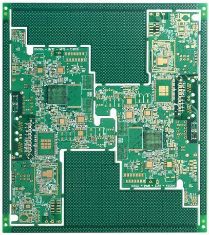
What is a Buried Via PCB?
A Buried Via PCB, also known as a sub-surface mounted via PCB, is a type of printed circuit board that features vias that are buried within the inner layers of the board. Unlike traditional through-hole vias, which go through all layers of the PCB, buried vias only connect the inner layers of the board, making them invisible from the surface.
Advantages of Buried Via PCBs
Buried Via PCBs offer several advantages over traditional PCBs:
- Space Savings: By burying the vias within the inner layers of the board, more space is available on the surface for components and routing.
- Improved Signal Integrity: Buried vias reduce the length of the signal path, which can improve signal integrity and reduce electromagnetic interference (EMI).
- Increased Reliability: Buried vias are less susceptible to mechanical stress and damage, which can increase the overall reliability of the PCB.
How are Buried Via PCBs Manufactured?
The manufacturing process for Buried Via PCBs is more complex than traditional PCBs. The process involves the following steps:
- Creating the Inner Layers: The inner layers of the PCB are created using standard PCB manufacturing techniques, such as etching and plating.
- Drilling the Vias: The vias are drilled into the inner layers of the board using a laser or mechanical drill.
- Filling the Vias: The vias are filled with a conductive material, such as copper or conductive epoxy, to create an electrical connection between the layers.
- Laminating the Layers: The inner layers are laminated together with the outer layers of the board using heat and pressure.
- Finishing the Board: The board is finished using standard PCB finishing techniques, such as solder mask and silkscreen.
Challenges of Manufacturing Buried Via PCBs
While Buried Via PCBs offer many advantages, they also present some challenges in manufacturing:
- Increased Cost: The additional steps involved in manufacturing Buried Via PCBs can increase the overall cost of the board.
- Longer Lead Times: The complex manufacturing process can also result in longer lead times compared to traditional PCBs.
- Limited Layer Count: The number of layers that can be used in a Buried Via PCB is limited by the manufacturing process and the capabilities of the PCB manufacturer.

Applications of Buried Via PCBs
Buried Via PCBs are used in a variety of applications where space savings, signal integrity, and reliability are critical. Some common applications include:
- Aerospace and Defense: Buried Via PCBs are often used in aerospace and defense applications where size and weight are critical factors.
- Medical Devices: Medical devices, such as implantable devices and wearable technology, often require small, reliable PCBs with high signal integrity.
- High-Speed Electronics: Buried Via PCBs are used in high-speed electronic applications, such as 5G communications and high-performance computing, where signal integrity is critical.
Comparison of Buried Via PCBs to Other PCB Types
| PCB Type | Advantages | Disadvantages |
|---|---|---|
| Buried Via PCB | Space savings, improved signal integrity, increased reliability | Increased cost, longer lead times, limited layer count |
| Through-Hole PCB | Low cost, easy to manufacture | Limited routing space, lower signal integrity |
| HDI PCB | High density, improved signal integrity | High cost, complex manufacturing process |
| Flex PCB | Flexibility, space savings | Limited layer count, higher cost |

Designing with Buried Via PCBs
When designing with Buried Via PCBs, there are several factors to consider:
- Layer Stack-Up: The layer stack-up of the board must be carefully designed to ensure proper connectivity between the inner layers and to minimize signal integrity issues.
- Via Placement: The placement of the vias must be carefully considered to ensure proper connectivity and to minimize signal integrity issues.
- Material Selection: The materials used in the PCB, such as the dielectric and the conductive material used in the vias, must be carefully selected to ensure proper performance and reliability.
Best Practices for Designing with Buried Via PCBs
To ensure successful design and manufacturing of Buried Via PCBs, follow these best practices:
- Work with an Experienced PCB Manufacturer: Choose a PCB manufacturer with experience in manufacturing Buried Via PCBs to ensure proper design and manufacturing.
- Use Simulation Tools: Use simulation tools to model the signal integrity and EMI performance of the board before manufacturing.
- Follow Design Guidelines: Follow the design guidelines provided by the PCB manufacturer to ensure proper design and manufacturing.

Future Trends in Buried Via PCBs
As technology continues to advance, the demand for smaller, more reliable PCBs with high signal integrity will continue to grow. Some future trends in Buried Via PCBs include:
- Increased Layer Count: As manufacturing processes improve, the number of layers that can be used in a Buried Via PCB will increase, allowing for even greater space savings and routing flexibility.
- Advanced Materials: New materials, such as low-loss dielectrics and high-performance conductive materials, will be developed to improve the performance and reliability of Buried Via PCBs.
- Automation: Automated design and manufacturing processes will be developed to reduce lead times and costs associated with Buried Via PCBs.
Conclusion
Buried Via PCBs offer many advantages over traditional PCBs, including space savings, improved signal integrity, and increased reliability. While they present some challenges in manufacturing and design, the benefits they offer make them an attractive option for many applications. As technology continues to advance, the demand for Buried Via PCBs will likely grow, and new manufacturing processes and materials will be developed to meet this demand.
FAQ
1. What is the difference between a Buried Via PCB and a traditional PCB?
A Buried Via PCB features vias that are buried within the inner layers of the board, while a traditional PCB has vias that go through all layers of the board.
2. What are the advantages of using a Buried Via PCB?
The advantages of using a Buried Via PCB include space savings, improved signal integrity, and increased reliability.
3. What are the challenges of manufacturing Buried Via PCBs?
The challenges of manufacturing Buried Via PCBs include increased cost, longer lead times, and limited layer count.
4. What are some common applications for Buried Via PCBs?
Common applications for Buried Via PCBs include aerospace and defense, medical devices, and high-speed electronics.
5. What are some best practices for designing with Buried Via PCBs?
Best practices for designing with Buried Via PCBs include working with an experienced PCB manufacturer, using simulation tools to model signal integrity and EMI performance, and following design guidelines provided by the PCB manufacturer.


Leave a Reply