Introduction
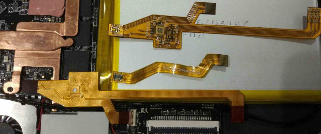
Flexible printed circuit boards (FPCBs) are ubiquitous in modern electronics. As devices continue to get smaller and more portable, flexible circuits enable efficient and reliable interconnections while allowing for mechanical flexibility and dynamic configurations.
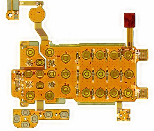
One area of innovation in FPCB technology is the development of multilayer flexible boards. Adding multiple conductive layers interconnected by plated through-holes increases circuit density and design options tremendously. Multilayer flexible PCBs enable highly complex circuits to be packaged in very compact form factors.
In this article, we will explore the key aspects of multilayer flexible PCB technology, including:
- Benefits of multilayer flex circuits
- Materials and construction
- Design considerations
- Manufacturing processes
- Emerging trends
Understanding multilayer flexible PCB technology is essential for engineers and product developers working on cutting-edge flexible electronics designs.
Benefits of Multilayer Flexible Circuits
Compared to single layer flex circuits, multilayer FPCBs provide:
- Higher circuit density: Multiple layers allow more components and traces to fit in a given area. Circuit density improves by 30-40% with each additional layer.
- Greater routing flexibility: With more layers, traces can take more direct routing paths between components, improving efficiency. Crossover connections are also easier with multiple layers.
- Improved impedance control: Ground planes and power planes can be incorporated to optimize impedances for high-speed signals.
- Embedded components: Passive components like resistors and capacitors can be embedded between layers, saving space.
- Design partitioning: Different sections of a complex circuit can be assigned to different layers for organization.
- Enhanced functionality: More layers allow more complex circuits with more capabilities and features.
| Benefit | Description |
|---|---|
| Higher circuit density | 30-40% increase in circuit density per layer added |
| Greater routing flexibility | More direct routing paths improve efficiency |
| Improved impedance control | Incorporate ground/power planes |
| Embedded components | Passives can be embedded between layers |
| Design partitioning | Assign circuit sections to different layers |
| Enhanced functionality | More complex circuits with more capabilities |
In short, multilayer flex provides design flexibility and miniaturization that is difficult to achieve with single layer boards. The tradeoff is increased complexity and cost.
Multilayer Flex Materials and Construction
The material system for a multilayer flex circuit includes:
- Flexible dielectric layers – Usually polyimide films like Kapton. Thickness ranges from 12.5-100μm.
- Adhesive layers – Bond the dielectric layers. Common adhesives are acrylic, epoxy, or polyimide.
- Conductive layers – Rolled annealed copper foil, typically 12-35μm thick.
- Cover layers – Protective coatings like solder mask, ink, or stiffeners.
The flexible layers are bonded together in a press using heat and pressure. Aligning the layers accurately is critical. Drilled or laser ablated through-holes interconnect the conductive layers. Plating makes the hole walls conductive.
FPCB suppliers offer many dielectric and adhesive options to suit different mechanical, electrical, and reliability requirements.
Construction Options
Rigid-flex – Combines flex layers with rigid FR4 layers for stiffness. Great for dynamic flexing parts like foldable devices.
Sculptured flex – Varies the thickness in certain areas by removing dielectric layers. Used to fit space constraints.
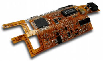
Embedded components – Passives like resistors and capacitors are built into the PCB layers. Saves space and cost.
Flexible chip packaging – Bare dice are mounted directly onto flex circuit layers, eliminating chip packaging. Extremely space efficient.
Design Considerations for Multilayer Flex
Designing a reliable, manufacturable multilayer flex board requires attention to:
- Layer stackup – Overall sequence and thickness of dielectric, adhesive, and copper layers. Definesmechancial and electrical properties.
- Material selection – Dielectric flexibility, adhesive bonding, copper weight, coverlay materials all affect performance.
- Bend radius – Minimum bend radius varies by layer stackup. Dynamic flexing needs more analysis.
- Routing – Escape routing from tight component pads can be challenging on flex boards. Requires planning.
- Component mounting – Direct component attach or sockets must accommodate flexing.
- Via construction – Plated through hole, blind, buried, filled, or microvia. Reliability varies.
- Thermal management – Flex boards can heat up quickly. May require openings or thermal vias.
- Modeling and Analysis – Use FEA and 3D modeling to predict stresses, flexibility, vibrations, etc.
Prototyping and testing is highly recommended to verify the design. Work closely with your flex PCB manufacturer during design to avoid manufacturability issues.
Manufacturing Multilayer Flexible Circuits
Producing multilayer flex boards requires specialized processes and equipment. Here are some key steps:
- Layer alignment – Conductive and dielectric layers are stacked and aligned with precision equipment. Alignment accuracy is critical.
- Bonding – Layers are bonded in a heated press via adhesive cured with heat and pressure. Parameters are carefully controlled.
- Via formation – Mechanical drilling or laser ablation creates through-holes for interlayer connections.
- Plating – Walls of holes are plated with copper to form conductive vias between layers.
- Etching – Unwanted copper is etched away to form the traces and pads. Photolithographic methods are typically used.
- Coverlay application – Protective solder mask and other coatings are applied to the outer layers.
- Component attachment – BGAs, flip chips, or other components are soldered or adhered.
- Testing and inspection – Rigorous electrical testing and optical inspection ensures quality.
The process is additive, building up the multilayer board layer-by-layer. Precision processes and exacting standards are required to produce defect-free multilayer flex PCBs.
Key Factors for Manufacturability
- Minimum trace/space capability
- Registration accuracy
- Aspect ratios of traces and gaps
- Flexibility and bending dynamics
- Drilling/ablating capability for dense microvias
- Fine line imaging and etching
- Dimensional stability of materials
- Handling thin/flexible materials
- Cleanliness and contamination control
Emerging Trends in Multilayer Flexible PCBs
Some leading edge developments in multilayer flex PCB technology include:
- Extreme layer counts – Flex boards with 20+ layers are being developed, enabling integration of complete systems.
- Flex-on-flex – Stacking flex boards vertically to form 3D interconnect structures. Enables flexiblestacked die packaging.
- Liquid crystal polymer (LCP) – A new advanced dielectric material with improved high frequency performance.
- Microflex – Features trace widths and spaces down to 15μm. Eliminates connectors for dense chip I/O.
- Stretchable circuits – Uses novel materials that allow flexible PCBs to stretch and compress dynamically.
- Additive processes – Additive manufacturing techniques like inkjet and aerosol printing are being adapted toflex board fabrication.
- Embedded actives and passives – Taking integrated circuit fabrication approaches to enableembedding active components like ICs inside flex layers.
These new technologies will open up exciting new possibilities for flexible printed circuit boards. Expect rapid evolution as advanced flex circuits power the connected world.
Multilayer Flexible PCBs – FAQ
Q: What are some typical applications for multilayer flex circuits?
A: Smartphones, wearable devices, medical electronics, automotive sensors, aerospace avionics, consumer gadgets, and robots/drones are common applications. Basically any product where flexibility, space, weight savings, or dynamic configurations are needed.
Q: How many layers can be produced in multilayer flex boards?
A: Currently 12 layers is typical, but flex PCBs with 20+ layers are feasible with microvia technology. The limit comes down to manufacturability factors like layer alignment tolerances and fine geometry etching.
Q: How are components mounted on multilayer flex circuits?
A: Surface mount pads allow soldering of standard SMT components. Flex-specific packages like Ball Grid Arrays (BGAs) or direct chip attach are popular for high density. Sockets are sometimes used to allow removable components.
Q: How small of a bend radius can multilayer flex boards handle?
A: It depends on the stackup, but bend radii down to a few mm are possible. Dynamic bend cycle life also depends on the materials used. Testing is required to qualify a design for flex reliability.
Q: What are some key differences when laying out multilayer flex PCBs versus rigid boards?
A: Trace geometry limitations, via construction, layer stackups, bend radius rules, copper relief patterns, handling ultra-thin layers, and dynamic flex effects like creep and stress relaxation. Work closely with your flex PCB supplier during design.


Leave a Reply