Introduction to Snubber Circuits
In the realm of electrical engineering, power surges pose a significant threat to electronic devices and systems. These sudden spikes in voltage or current can cause irreparable damage to components, leading to malfunctions and even complete failures. To mitigate these risks, engineers employ various protective measures, one of which is the implementation of snubber circuits. In this comprehensive article, we will delve into the world of snubber circuits, exploring their functionality, types, applications, and design considerations.
What is a Snubber Circuit?
A snubber circuit, also known as a snubber network, is an electronic circuit designed to suppress voltage spikes or limit the rate of change of voltage (dV/dt) across a load. Its primary purpose is to protect sensitive components, such as transistors, thyristors, and switches, from the harmful effects of power surges. By absorbing excess energy and controlling the rise and fall times of voltage waveforms, snubber circuits enhance the reliability and longevity of electronic systems.
The Need for Snubber Circuits
Power surges can originate from various sources, including:
- Switching transients: When inductive loads, such as motors or transformers, are switched on or off, they generate voltage spikes due to the sudden change in current.
- Electromagnetic interference (EMI): External electromagnetic fields can induce voltage spikes in electronic circuits.
- Power line disturbances: Lightning strikes, power grid fluctuations, and load switching can cause power surges on the supply lines.
These power surges can lead to the following issues:
- Component breakdown: Excessive voltage or current can cause components to fail prematurely or even instantaneously.
- Insulation damage: High voltage spikes can deteriorate the insulation of wires and components, leading to short circuits and safety hazards.
- Electromagnetic interference: Power surges can generate EMI, which can disrupt the operation of nearby electronic devices.
To address these challenges, snubber circuits are employed as a protective measure.
Types of Snubber Circuits
Snubber circuits can be classified into two main categories based on their purpose and design: RC snubbers and RCD snubbers.
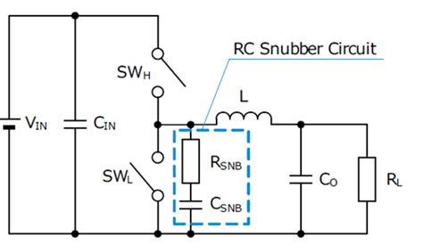
RC Snubber Circuits
An RC snubber circuit consists of a resistor (R) and a capacitor (C) connected in series across the load. The resistor limits the peak current during the initial charging of the capacitor, while the capacitor absorbs the energy associated with voltage spikes. When a voltage spike occurs, the capacitor quickly charges, preventing the voltage across the load from rising too rapidly. The resistor then dissipates the stored energy as heat during the discharge phase.
The values of the resistor and capacitor in an RC snubber circuit are chosen based on the following factors:
- Load characteristics: The resistor value should be high enough to limit the peak current but low enough to allow the capacitor to charge quickly. The capacitor value should be sufficient to absorb the expected energy of the voltage spikes.
- Switching frequency: Higher switching frequencies require lower capacitor values to ensure quick charging and discharging.
- Voltage and current ratings: The resistor and capacitor must be rated to withstand the maximum expected voltage and current levels.
RC snubber circuits are commonly used in applications such as:
- Power supply circuits: To suppress voltage spikes caused by the switching of rectifiers or transformers.
- Motor drives: To protect power electronic switches, such as MOSFETs or IGBTs, from voltage spikes during motor startup or braking.
- Relay contacts: To minimize contact arcing and extend the life of relay contacts.
RCD Snubber Circuits
An RCD snubber circuit, also known as a rate-of-rise snubber, consists of a resistor (R), a capacitor (C), and a diode (D) connected in a specific configuration across the load. The resistor and capacitor are connected in series, while the diode is connected in parallel with the resistor. The purpose of an RCD snubber is to limit the rate of rise of voltage (dV/dt) across the load during switching transitions.
When the voltage across the load starts to rise rapidly, the capacitor in the RCD snubber circuit begins to charge through the resistor. The charging current is limited by the resistor, effectively controlling the rate of voltage rise. Once the voltage reaches its steady-state value, the diode becomes forward-biased, providing a low-impedance path for the capacitor to discharge. This discharging process helps to dissipate the stored energy and reset the snubber for the next switching event.
The selection of components for an RCD snubber circuit involves the following considerations:
- dV/dt limit: The resistor and capacitor values should be chosen to limit the rate of voltage rise to a safe level for the protected components.
- Peak current: The resistor value should be high enough to limit the peak current through the capacitor and diode during the charging phase.
- Power dissipation: The resistor must be capable of dissipating the energy stored in the capacitor during each switching cycle.
- Diode ratings: The diode should have a sufficient voltage rating to withstand the maximum expected voltage across the load and a current rating to handle the discharge current of the capacitor.
RCD snubber circuits find applications in various power electronic systems, such as:
- Switching power supplies: To reduce voltage stress on power switches and minimize electromagnetic interference (EMI).
- Inductive load switching: To protect switches and reduce contact arcing when switching inductive loads, such as solenoids or relays.
- Thyristor circuits: To control the rate of voltage rise across thyristors during turn-off, preventing false triggering.

Designing Snubber Circuits
The design of a snubber circuit involves selecting the appropriate components and determining their values based on the specific requirements of the application. The following steps outline the general design process for snubber circuits:
- Identify the critical parameters:
- Maximum expected voltage spike amplitude
- Maximum allowable rate of voltage rise (dV/dt)
- Switching frequency
-
Load characteristics (e.g., inductance, capacitance)
-
Choose the snubber circuit topology:
- RC snubber for voltage spike suppression
-
RCD snubber for dV/dt limitation
-
Calculate the component values:
- For an RC snubber:
- Select the capacitor value based on the energy to be absorbed
- Determine the resistor value to limit the peak current and ensure proper charging/discharging
-
For an RCD snubber:
- Select the capacitor value based on the desired dV/dt limit
- Calculate the resistor value to control the charging current and power dissipation
- Choose the diode based on voltage and current ratings
-
Verify the design:
- Simulate the circuit using software tools to assess its performance
-
Prototype the circuit and conduct real-world testing to validate its effectiveness
-
Optimize and refine:
- Fine-tune component values based on simulation and test results
- Consider factors such as component tolerances, temperature effects, and long-term reliability
It is important to note that the design of snubber circuits often involves trade-offs between performance, cost, and size. Engineers must strike a balance between these factors to achieve the desired level of protection while meeting the constraints of the application.

Snubber Circuit Applications
Snubber circuits find extensive use in various domains of electrical and electronic engineering. Some common applications include:
Power Electronics
In power electronic systems, such as switched-mode power supplies (SMPS), motor drives, and inverters, snubber circuits play a crucial role in protecting power switches (e.g., MOSFETs, IGBTs) from voltage spikes and limiting dV/dt during switching transitions. By reducing voltage stress and minimizing EMI, snubber circuits contribute to the reliability and efficiency of power conversion processes.
Automotive Electronics
In automotive applications, snubber circuits are employed to protect sensitive electronic components from the harsh electrical environment. They are used in various systems, such as ignition systems, fuel injectors, and motor control units, to suppress voltage spikes caused by inductive loads and ensure the reliable operation of electronic control modules (ECMs).
Industrial Control Systems
Industrial control systems often involve the switching of inductive loads, such as motors, solenoids, and relays. Snubber circuits are used to minimize contact arcing, reduce electromagnetic interference, and extend the life of switching devices. They are commonly found in motor starters, contactors, and programmable logic controllers (PLCs).
Telecommunications
In telecommunications equipment, such as modems, routers, and switches, snubber circuits are employed to protect sensitive electronic components from voltage spikes and transients. They help to ensure the integrity of data transmission and prevent damage to communication interfaces, such as Ethernet ports and telephone lines.
Medical Electronics
Medical electronic devices, such as patient monitoring systems, imaging equipment, and surgical instruments, rely on snubber circuits to ensure safe and reliable operation. Snubber circuits protect sensitive electronic components from voltage spikes and transients that may arise from the switching of inductive loads or external electromagnetic interference.

Snubber Circuit Maintenance and Troubleshooting
To ensure the continued effectiveness of snubber circuits, regular maintenance and troubleshooting are essential. The following practices can help maintain the performance and reliability of snubber circuits:
-
Visual inspection: Regularly inspect the snubber circuit components for signs of physical damage, such as cracks, burns, or discoloration. Replace any damaged components promptly.
-
Electrical testing: Periodically measure the resistance, capacitance, and diode forward voltage drop of the snubber circuit components to ensure they are within the specified tolerances. Use a multimeter or an LCR meter for accurate measurements.
-
Waveform analysis: Use an oscilloscope to observe the voltage and current waveforms across the load and the snubber circuit. Look for any abnormalities, such as excessive ringing, overshoot, or undershoot, which may indicate a malfunctioning snubber or underlying issues in the system.
-
Thermal monitoring: Monitor the temperature of the snubber circuit components, especially the resistor, which dissipates energy as heat. Excessive temperature rise may indicate overloading or inadequate heat dissipation, requiring further investigation and corrective action.
-
Preventive replacement: In critical applications or environments with high levels of stress, consider replacing snubber circuit components proactively based on the manufacturer’s recommendations or the system’s maintenance schedule.
When troubleshooting snubber circuits, consider the following steps:
- Verify the correct installation and connections of the snubber circuit components.
- Check for any loose or damaged connections that may affect the circuit’s performance.
- Measure the voltage and current waveforms across the load and compare them with the expected values.
- Analyze the waveforms for any signs of excessive voltage spikes, ringing, or inadequate suppression.
- If the snubber circuit appears to be ineffective, review the design calculations and component selections to ensure they are appropriate for the application.
- Consider external factors, such as EMI sources or load variations, that may be contributing to the problem.
By following these maintenance and troubleshooting practices, engineers can ensure that snubber circuits continue to provide reliable protection against power surges and maintain the overall health of electronic systems.
Frequently Asked Questions (FAQ)
-
What is the purpose of a snubber circuit?
A snubber circuit is designed to protect electronic components from voltage spikes and limit the rate of change of voltage (dV/dt) across a load. It suppresses power surges and extends the life of sensitive components. -
What are the two main types of snubber circuits?
The two main types of snubber circuits are RC snubbers and RCD snubbers. RC snubbers are used for voltage spike suppression, while RCD snubbers are used for dV/dt limitation. -
How do I select the component values for a snubber circuit?
The selection of component values for a snubber circuit depends on factors such as the maximum expected voltage spike amplitude, the maximum allowable rate of voltage rise (dV/dt), switching frequency, and load characteristics. It involves calculations based on the energy to be absorbed and the desired dV/dt limit. -
Can a snubber circuit completely eliminate voltage spikes?
While snubber circuits are effective in suppressing voltage spikes and limiting dV/dt, they cannot completely eliminate them. The effectiveness of a snubber circuit depends on its design and the specific application requirements. -
How often should I perform maintenance on snubber circuits?
The frequency of maintenance for snubber circuits depends on the application and the operating environment. In general, it is recommended to perform visual inspections, electrical testing, and waveform analysis periodically to ensure the snubber circuit components are functioning correctly. In critical applications or harsh environments, preventive replacement of components may be necessary based on the manufacturer’s recommendations or the system’s maintenance schedule.
Conclusion
Snubber circuits play a vital role in protecting electronic systems from the detrimental effects of power surges. By suppressing voltage spikes and limiting the rate of change of voltage, snubber circuits enhance the reliability, efficiency, and longevity of electronic components. Understanding the types, design considerations, and applications of snubber circuits is crucial for engineers to effectively implement these protective measures in various domains, ranging from power electronics to medical devices.
As technology advances and the complexity of electronic systems increases, the importance of snubber circuits will only continue to grow. By staying informed about the latest developments in snubber circuit design and applying best practices in maintenance and troubleshooting, engineers can ensure that electronic systems remain safe, reliable, and resilient in the face of power surges.
In conclusion, snubber circuits are an indispensable tool in the arsenal of electrical and electronic engineers. By providing a robust defense against power surges, they contribute to the overall performance and longevity of electronic systems, enabling them to operate safely and efficiently in a wide range of applications.


Leave a Reply