Introduction to PCB Assembly
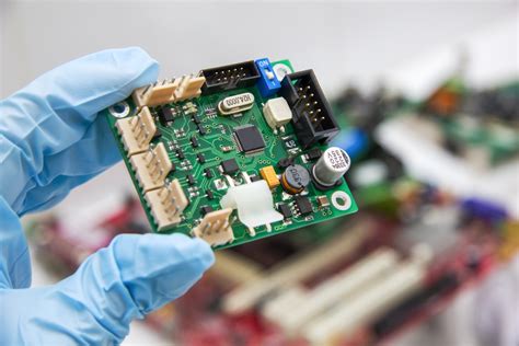
PCB (Printed Circuit Board) assembly is the process of attaching electronic components to a printed circuit board to create a functional electronic device. The PCB serves as the foundation for the electronic components, providing mechanical support and electrical connections between them. PCB assembly is a crucial step in the manufacturing of electronic devices, from simple consumer gadgets to complex industrial equipment.
What is a Printed Circuit Board (PCB)?
A Printed Circuit Board (PCB) is a thin board made of fiberglass or other composite material, with conductive tracks, pads, and other features etched from copper sheets laminated onto the board. These copper tracks and pads form the electrical connections between the various components that will be attached to the board during the assembly process.
PCBs come in various types, depending on the number of layers and the density of the components:
| PCB Type | Description |
|---|---|
| Single-sided PCB | Components are placed on one side of the board, with conductive tracks on the opposite side. |
| Double-sided PCB | Components and conductive tracks are placed on both sides of the board. |
| Multi-layer PCB | Consists of three or more conductive layers, allowing for more complex designs and higher component density. |
Components Used in PCB Assembly
The components used in PCB assembly can be broadly categorized into two types:
-
Through-hole components: These components have long leads that are inserted into holes drilled in the PCB and soldered to pads on the opposite side of the board.
-
Surface mount components: These components are smaller and have short leads or no leads at all. They are soldered directly onto pads on the surface of the PCB.
Some common components used in PCB assembly include:
- Resistors
- Capacitors
- Inductors
- Diodes
- Transistors
- Integrated Circuits (ICs)
- Connectors
- Switches
PCB Assembly Process
The PCB assembly process involves several steps, each of which requires precision and attention to detail to ensure the final product functions as intended.
Step 1: Solder Paste Application
The first step in PCB assembly is applying solder paste to the pads on the PCB where the surface mount components will be placed. This is typically done using a stencil and a solder paste printer. The stencil is a thin metal sheet with openings that correspond to the pads on the PCB. The solder paste is spread over the stencil, filling the openings and depositing the paste onto the pads.
Step 2: Component Placement
Once the solder paste has been applied, the surface mount components are placed onto the pads using a pick-and-place machine. This machine uses a vacuum nozzle to pick up the components from a tray and place them onto the PCB with high precision. The machine is programmed with the coordinates of each component’s location on the board.
Step 3: Reflow Soldering
After the components have been placed, the PCB goes through a reflow soldering process. The board is passed through a reflow oven, which heats the solder paste, causing it to melt and form a permanent bond between the components and the pads. The temperature profile of the reflow process is carefully controlled to ensure that the components are not damaged by excessive heat.
Step 4: Through-Hole Component Insertion and Wave Soldering
If the PCB design includes through-hole components, these are inserted into the holes on the board manually or using an automated insertion machine. Once the through-hole components are in place, the board undergoes a wave soldering process. The board is passed over a molten solder wave, which fills the holes and creates a connection between the component leads and the pads on the opposite side of the board.
Step 5: Inspection and Testing
After the soldering processes are complete, the PCB undergoes a visual inspection to check for any defects, such as bridging (unintended connections between pads), solder balls, or missing components. Automated optical inspection (AOI) systems are often used to speed up this process and ensure consistency.
Following the visual inspection, the PCB is subjected to various electrical tests to verify its functionality. These tests may include:
- Continuity testing
- Insulation resistance testing
- In-circuit testing
- Functional testing
Step 6: Conformal Coating and Final Assembly
Depending on the application and the environment in which the electronic device will be used, a conformal coating may be applied to the PCB to protect it from moisture, dust, and other contaminants. This coating is typically a thin layer of polymer material that conforms to the shape of the components and the board.
Finally, the PCB is integrated into the final product, which may involve enclosures, cabling, and other mechanical assembly processes.

PCB Assembly Techniques
There are two main techniques used in PCB assembly: through-hole and surface mount.
Through-Hole Assembly
Through-hole assembly involves inserting the leads of components through holes drilled in the PCB and soldering them to pads on the opposite side of the board. This technique is generally used for larger components or those that require more mechanical stability.
Advantages of through-hole assembly:
– Stronger mechanical bonds between components and the board
– Easier to replace or repair components
– Better for high-power applications
Disadvantages of through-hole assembly:
– Larger component size and board space requirements
– Slower assembly process compared to surface mount
– Higher cost for high-volume production
Surface Mount Assembly
Surface mount assembly involves placing components directly onto pads on the surface of the PCB and soldering them in place. This technique allows for smaller components and higher component density on the board.
Advantages of surface mount assembly:
– Smaller component size and higher component density
– Faster assembly process
– Lower cost for high-volume production
Disadvantages of surface mount assembly:
– More difficult to replace or repair components
– Requires more precise placement and soldering equipment
– More susceptible to thermal stress and vibration

Factors Affecting PCB Assembly Quality
Several factors can influence the quality of the PCB assembly process:
-
Design for Manufacturing (DFM): The PCB design should follow DFM guidelines to ensure that the board can be manufactured and assembled efficiently and reliably. This includes considerations such as component spacing, pad sizes, and soldermask design.
-
Component quality: The quality of the components used in the assembly process can have a significant impact on the overall quality of the final product. It is essential to source components from reputable suppliers and to perform incoming quality control inspections.
-
Solder paste quality: The quality of the solder paste used in the assembly process can affect the reliability of the solder joints. Factors such as the composition of the solder paste, its viscosity, and its storage conditions should be carefully controlled.
-
Reflow profile: The temperature profile used during the reflow soldering process must be carefully optimized to ensure that the solder paste melts and flows properly without damaging the components or the board.
-
Inspection and testing: Thorough inspection and testing procedures are essential for identifying and correcting any defects in the assembled PCB. This includes visual inspection, automated optical inspection (AOI), and various electrical tests.

PCB Assembly Challenges and Solutions
PCB assembly can present several challenges, particularly as electronic devices become more complex and miniaturized. Some common challenges and their solutions include:
-
Miniaturization: As components become smaller, placing and soldering them onto the PCB becomes more difficult. This can be addressed through the use of advanced pick-and-place machines and high-precision soldering equipment.
-
High-density designs: As component density on PCBs increases, the risk of signal integrity issues and electromagnetic interference (EMI) also increases. This can be mitigated through careful design practices, such as proper grounding, shielding, and the use of high-quality materials.
-
Thermal management: High-power components can generate significant amounts of heat, which can affect the reliability of the PCB and surrounding components. Thermal management techniques, such as the use of heatsinks, thermal vias, and thermal interface materials, can help dissipate heat effectively.
-
Rework and repair: Reworking or repairing surface mount components can be challenging due to their small size and close proximity to other components. Specialized tools, such as hot air rework stations and microscopes, can facilitate these processes.
-
Supply chain management: Ensuring a reliable supply of components and materials is crucial for maintaining the quality and consistency of PCB assembly. This can be achieved through effective supplier management, inventory control, and regular communication with suppliers.
Frequently Asked Questions (FAQ)
-
What is the difference between PCB fabrication and PCB assembly?
PCB fabrication is the process of creating the bare PCB, which involves designing the circuit, creating the artwork, and etching the copper traces onto the board. PCB assembly is the process of attaching the electronic components to the fabricated PCB. -
What is the difference between through-hole and surface mount components?
Through-hole components have long leads that are inserted into holes drilled in the PCB and soldered to pads on the opposite side. Surface mount components are smaller and have short leads or no leads at all, and they are soldered directly onto pads on the surface of the PCB. -
What is solder paste, and how is it applied to the PCB?
Solder paste is a mixture of tiny solder particles suspended in a flux medium. It is applied to the pads on the PCB using a stencil and a solder paste printer before the surface mount components are placed. -
What is reflow soldering, and how does it work?
Reflow soldering is a process used to solder surface mount components to the PCB. The PCB with the solder paste and components is passed through a reflow oven, which heats the solder paste, causing it to melt and form a permanent bond between the components and the pads. -
What is the purpose of conformal coating in PCB assembly?
Conformal coating is a thin layer of polymer material applied to the assembled PCB to protect it from moisture, dust, and other contaminants. It helps to improve the reliability and longevity of the electronic device, especially in harsh environments.
Conclusion
PCB assembly is a critical process in the manufacturing of electronic devices, involving the attachment of components to a printed circuit board. Understanding the basics of PCB assembly, including the components, techniques, and factors affecting quality, is essential for anyone involved in electronics design or manufacturing.
By following best practices in PCB design, component selection, and assembly processes, and by staying informed about the latest technologies and techniques, you can ensure the production of high-quality, reliable electronic devices. As electronic devices continue to evolve and become more complex, the importance of skilLED PCB Assembly will only continue to grow.


Leave a Reply