What is a Rigid PCB?
A Rigid PCB, or Printed Circuit Board, is a flat board made of insulating material with copper traces printed on it to connect electronic components. It is called “rigid” because the board is made of a solid, non-flexible material, usually a glass-reinforced epoxy laminate called FR-4.
Rigid PCBs are the foundation of most electronic devices, from smartphones and computers to medical equipment and aerospace systems. They provide a stable platform for mounting and interconnecting various components such as resistors, capacitors, integrated circuits (ICs), and connectors.
Key Characteristics of Rigid PCBs
- Material: FR-4 is the most common material used for rigid PCBs due to its excellent mechanical and electrical properties, as well as its affordability.
- Copper Layers: Rigid PCBs can have one or multiple copper layers, depending on the complexity of the circuit design. The number of layers can range from single-sided (one layer) to multi-layer boards with 8, 16, or even more layers.
- Thickness: The thickness of a rigid PCB is typically measured in millimeters (mm) and can vary depending on the application and the number of layers. Common thicknesses include 0.8mm, 1.6mm, and 2.4mm.
- Durability: Rigid PCBs are known for their durability and ability to withstand various environmental factors such as temperature, humidity, and vibration.
Advantages of Rigid PCBs
Rigid PCBs offer several advantages over other types of circuit boards, making them the preferred choice for many applications:
- Reliability: The solid construction of rigid PCBs ensures a high level of reliability, even in harsh operating conditions.
- High Density: Multi-layer rigid PCBs allow for high component density, enabling the design of compact and complex electronic devices.
- Excellent Heat Dissipation: The FR-4 material and copper layers provide good thermal conductivity, helping to dissipate heat generated by components.
- Cost-effective: Rigid PCBs are generally more affordable than flexible or rigid-flex PCBs, especially for high-volume production.

Rigid PCB Manufacturing Process
The manufacturing process for rigid PCBs involves several steps:
- Design: The PCB design is created using Electronic Design Automation (EDA) software, which generates the necessary files for manufacturing, such as Gerber files and drill files.
- Printing: The PCB design is printed onto a photosensitive film or directly onto the copper-clad laminate using a photoplotter or direct imaging machine.
- Etching: The exposed copper is etched away using a chemical solution, leaving only the desired copper traces.
- Drilling: Holes are drilled through the board to accommodate through-hole components and vias (vertical interconnect access).
- Plating: A thin layer of copper is electroplated onto the board to provide electrical continuity between layers and to protect the exposed copper traces.
- Solder Mask and Silkscreen: A solder mask is applied to the board to insulate the copper traces and prevent short circuits. A silkscreen layer is then added to label components and provide assembly instructions.
- Surface Finish: A surface finish, such as HASL (Hot Air Solder Leveling), ENIG (Electroless Nickel Immersion Gold), or OSP (Organic Solderability Preservative), is applied to protect the exposed copper and enhance solderability.

Designing a Rigid PCB
Designing a rigid PCB requires knowledge of electronic circuits, PCB layout principles, and manufacturing constraints. Here are some key considerations when designing a rigid PCB:
- Schematic Design: Create a schematic diagram that represents the electrical connections between components. Ensure that the schematic is accurate and follows best practices for circuit design.
- Component Selection: Choose components that meet the requirements of your application, considering factors such as power rating, package size, and availability.
- PCB Layout: Arrange the components on the board and route the traces to create the physical layout of the PCB. Follow PCB layout guidelines to minimize signal integrity issues, such as crosstalk and electromagnetic interference (EMI).
- Manufacturing Constraints: Consider the limitations of the PCB manufacturing process, such as minimum trace width, minimum drill size, and clearance requirements. Consult with your PCB manufacturer to ensure that your design is manufacturable.
- Design for Assembly (DFA): Design the PCB with assembly in mind, considering factors such as component orientation, solder mask openings, and silkscreen markings to facilitate the assembly process.
PCB Layout Guidelines
To ensure a successful PCB layout, follow these general guidelines:
- Component Placement: Place components in a logical and organized manner, considering signal flow and power distribution. Keep related components close together to minimize trace lengths.
- Trace Routing: Route traces as directly as possible, avoiding sharp angles and long parallel runs. Use appropriate trace widths based on the current requirements of the circuit.
- Ground Plane: Use a solid ground plane to provide a low-impedance return path for signals and to minimize EMI.
- Decoupling Capacitors: Place decoupling capacitors close to the power pins of ICs to suppress high-frequency noise and maintain power integrity.
- Via Placement: Use vias strategically to connect traces between layers, but avoid placing them in high-speed signal paths or under components.
- Thermal Management: Consider the thermal requirements of components and provide adequate copper area for heat dissipation, if necessary.

Types of Rigid PCBs
Rigid PCBs can be categorized based on the number of copper layers and their construction:
- Single-sided PCB: A PCB with components and copper traces on only one side of the board.
- Double-sided PCB: A PCB with components and copper traces on both sides of the board.
- Multi-layer PCB: A PCB with three or more copper layers, separated by insulating layers. The layers are interconnected using vias.
- High Tg PCB: A PCB made with a high glass transition temperature (Tg) material, such as polyimide, for applications that require higher temperature resistance.
- Thick Copper PCB: A PCB with thicker copper layers (typically 3 oz or more) for high-current applications or improved thermal management.
| PCB Type | Layers | Typical Applications |
|---|---|---|
| Single-sided PCB | 1 | Simple, low-cost devices (e.g., toys, basic electronics) |
| Double-sided PCB | 2 | More complex devices (e.g., power supplies, amplifiers) |
| Multi-layer PCB | 3+ | High-density, complex devices (e.g., smartphones, computers) |
| High Tg PCB | Varies | Automotive, aerospace, and high-temperature applications |
| Thick Copper PCB | Varies | Power electronics, high-current applications |
Rigid PCB Testing and Inspection
To ensure the quality and reliability of rigid PCBs, various testing and inspection methods are employed:
- Visual Inspection: A manual or automated visual inspection of the PCB to check for obvious defects, such as missing components, solder bridges, or damaged traces.
- Automated Optical Inspection (AOI): An automated system that uses cameras and image processing software to detect manufacturing defects, such as component misalignment or incorrect polarity.
- X-ray Inspection: A non-destructive testing method that uses X-rays to reveal internal defects, such as voids in solder joints or broken vias.
- In-Circuit Testing (ICT): A test method that uses a bed-of-nails fixture to make electrical contact with test points on the PCB, allowing for the verification of component values and Circuit Continuity.
- Functional Testing: A test method that verifies the functionality of the assembled PCB by applying input signals and measuring output responses.
Applications of Rigid PCBs
Rigid PCBs find applications in a wide range of industries and products:
- Consumer Electronics: Smartphones, tablets, laptops, televisions, and home appliances.
- Automotive: Engine control units, infotainment systems, and advanced driver assistance systems (ADAS).
- Medical Devices: Diagnostic equipment, patient monitoring systems, and implantable devices.
- Industrial Automation: Programmable logic controllers (PLCs), sensors, and motor drives.
- Aerospace and Defense: Avionics, radar systems, and satellite communication equipment.
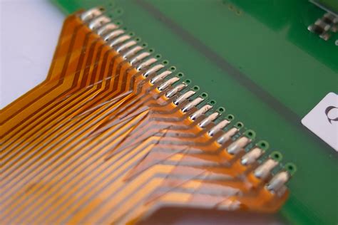
Rigid PCB vs. Flexible PCB
While rigid PCBs are the most common type of PCB, flexible PCBs offer unique advantages in certain applications:
| Feature | Rigid PCB | Flexible PCB |
|---|---|---|
| Flexibility | No flexibility, fixed shape | Can bend and flex, conformable to shapes |
| Durability | High, resistant to mechanical stress | Lower, can be prone to fatigue over time |
| Cost | Generally lower cost | Higher cost due to specialized materials |
| Size and Weight | Larger and heavier | Smaller and lighter |
| Applications | Most common electronics | Wearables, medical devices, tight spaces |
Future Trends in Rigid PCBs
As electronic devices continue to advance, rigid PCBs are evolving to meet new challenges:
- High-Speed Design: With increasing data rates and signal frequencies, PCB designers must employ advanced techniques to maintain signal integrity and minimize EMI.
- Miniaturization: The demand for smaller and more compact devices is driving the development of high-density interconnect (HDI) PCBs, which feature finer traces and smaller vias.
- Thermal Management: As power densities increase, PCBs must be designed with better thermal management solutions, such as metal-core PCBs or embedded heat pipes.
- Environmental Sustainability: There is a growing focus on using eco-friendly materials and processes in PCB manufacturing, such as lead-free solders and halogen-free laminates.
Frequently Asked Questions (FAQ)
-
What is the difference between a rigid PCB and a flexible PCB?
A rigid PCB is made of a solid, non-flexible material, while a flexible PCB is made of a thin, flexible substrate that can bend and conform to shapes. -
How many layers can a rigid PCB have?
A rigid PCB can have anywhere from one to multiple layers, with common configurations being single-sided, double-sided, and multi-layer (4, 6, 8, or more layers). -
What is the most common material used for rigid PCBs?
The most common material used for rigid PCBs is FR-4, a glass-reinforced epoxy laminate. -
What are the advantages of using a multi-layer rigid PCB?
Multi-layer rigid PCBs offer several advantages, including higher component density, better signal integrity, and improved EMI performance. -
How can I ensure my rigid PCB design is manufacturable?
To ensure your rigid PCB design is manufacturable, follow PCB layout guidelines, consider manufacturing constraints, and consult with your PCB manufacturer early in the design process.
Conclusion
Rigid PCBs are the backbone of modern electronics, providing a reliable and cost-effective solution for interconnecting components in a wide range of applications. By understanding the fundamentals of rigid PCBs, including their construction, manufacturing process, and design considerations, beginners can create successful PCB designs that meet the requirements of their projects.
As technology advances, rigid PCBs will continue to evolve, incorporating new materials, manufacturing techniques, and design strategies to enable the next generation of electronic devices.


Leave a Reply