What is SMT PCB Assembly?
SMT PCB Assembly, or Surface Mount Technology Printed Circuit Board assembly, is a method for producing electronic circuits in which the components are mounted directly onto the surface of printed circuit boards (PCBs). SMT has largely replaced the through-hole technology construction method of fitting components with wire leads into holes in the circuit board. Both technologies can be used on the same board for components not suited to surface mounting such as transformers and heat-sinked power semiconductors.
SMT PCB assembly is used in nearly all commercially produced electronics today, and has several advantages over through-hole mounting:
- Smaller components can be used, allowing for more compact designs
- Components can be mounted on both sides of the board
- Higher component density leads to smaller PCB size
- Faster and more automated assembly process
- Lower initial cost and time of setting up for production
- Fewer holes need to be drilled through the PCB
- Simpler and faster automated assembly
- Solder joints are more reliable due to improved manufacturing processes
- Better mechanical performance under shake and vibration conditions
However, SMT PCB assembly does have some disadvantages compared to through-hole mounting:
- Manual prototype assembly and component removal can be more difficult
- SMDs cannot be used directly with plug-in breadboards
- SMT parts generally cost more than equivalent through-hole parts
- SMDs are more difficult to inspect visually
- Equipment and training for manual assembly is more specialized and expensive
SMT PCB Assembly Process Overview
The SMT PCB assembly process consists of several key steps:
- Solder Paste Printing
- Pick and Place
- Reflow Soldering
- Inspection and Quality Control
1. Solder Paste Printing
The first step in SMT PCB assembly is applying solder paste to the board. Solder paste is a mixture of tiny solder balls and flux that helps the solder flow and adhere properly to the pads.
A solder paste stencil is placed over the PCB. The stencil is a thin sheet of stainless steel or nickel with laser-cut holes that correspond to the pads on the PCB where the solder paste needs to be applied.
The solder paste is then spread across the stencil using a squeegee blade, forcing it through the holes and onto the pads. The stencil is then removed, leaving precise deposits of solder paste on the PCB pads.
Key factors in the solder paste printing process include:
- Stencil thickness – Typically ranges from 0.1mm to 0.3mm (4-12 mils). Thicker stencils deposit more solder paste.
- Aperture size and shape – The holes in the stencil must be the right size and shape to deposit the proper amount of paste on each pad without forming bridges.
- Paste properties – The solder paste’s viscosity, particle size, flux type, and other properties affect how easily it rolls off the stencil and how well it prints.
- Squeegee pressure, speed, and angle – Must be optimized to force paste through the apertures cleanly and evenly without smearing.
- Snap-off distance – The small gap between the stencil and PCB as the squeegee passes. Typically 0.05-0.2 mm (2-8 mils).
- Board support and clamping – The PCB must be held completely flat and still to maintain proper alignment and contact with the stencil.
After printing, the PCB goes through a solder paste inspection (SPI) to check the volume, height, area, and alignment of the deposits.
2. Pick and Place
The next step is placing all the SMT components onto their respective pads on the PCB. This is done by automated pick and place machines.
The components, which come packaged in reels, trays, tubes, or sticks, are loaded into feeders on the machine. A computer program tells the machine where to place each part on the board.
High-speed pick and place machines use a vacuum head on a gantry system to rapidly pick up parts, rotate them to the proper orientation, and accurately place them on the PCB at rates up to tens of thousands of parts per hour. They can have multiple nozzles to pick and place several components at a time.
Smaller desktop pick and place machines are also available for prototype and low volume production.
Some key parameters in pick and place are:
- Placement Accuracy – How precisely the machine can place the parts. Typically ±0.05mm (2 mils) or better.
- Placement Rate – How many components the machine can place per hour. Ranges from a few hundred to over 100,000.
- Component Size Range – The minimum and maximum size of components the machine can handle, based on the nozzle sizes and part feeders available.
- Vision Capability – optical systems to detect fiducials for board alignment, recognize components, and measure placement accuracy.
After placement, an automated optical inspection (AOI) is often used to verify that all the parts are present and aligned correctly before soldering.
3. Reflow Soldering
After the components are placed, the PCB goes through a reflow oven to permanently solder the parts to the board.
The reflow oven has multiple temperature zones that the board passes through, typically via a conveyor belt. The heat melts the solder balls in the paste, which then cool and solidify to form a permanent mechanical and electrical connection.
The reflow oven temperature profile must be carefully controlled to ensure proper wetting of the solder without damaging the components or PCB. A typical lead-free reflow profile looks like this:
| Zone | Temperature | Time |
|---|---|---|
| Preheat | 150-180°C | 60-120 sec |
| Soak | 180-200°C | 60-120 sec |
| Reflow | 240-250°C | 30-60 sec |
| Cooling | < 100°C | 30-90 sec |
During the preheat and soak stages, the flux activates to clean the metal surfaces, remove oxides, and prevent further oxidation. The solder balls melt and wet the surfaces during the brief reflow stage at the peak temperature. During cooling, the molten solder solidifies into reliable intermetallic bonds.
Some of the key process variables in reflow soldering are:
- Peak Temperature – The maximum temperature reached during reflow. Must be high enough to fully melt the solder but not so high as to damage components.
- Time Above Liquidus (TAL) – How long the solder stays molten above its melting point. Typically 30-90 seconds.
- Ramp Rate – How quickly the temperature increases toward the peak. Typically 0.5-2°C/sec. Slower rates allow for more gentle heating and better activation of the flux.
- Atmosphere – Reflow can be done in air or under nitrogen. Nitrogen helps reduce oxidation for better solder wetting.
- Cooling Rate – How fast the board cools after reflow. Slow cooling promotes even joint solidification and reduces thermal stress. Forced air cooling may be used.
The reflow profile has to be matched to the thermal mass of the board, the heat sensitivity of the components, and the solder paste composition. Optimization often requires some trial and error.
4. Inspection and Quality Control
After the SMT PCB assembly process is complete, the boards need to be inspected and tested to ensure quality before they can be shipped.
Visual Inspection
The first quality check is usually a visual inspection by a human operator, looking for missing components, torn or lifted pads, misaligned parts, solder bridges, incomplete reflow, and other defects. A magnifying glass, stereo microscope, or digital microscope may be used for closer examination.
Automated Optical Inspection (AOI)
Automated optical inspection systems use cameras and image processing software to rapidly check PCB assembly quality. They can compare the actual board to the CAD data to verify the presence, position, polarity, and alignment of components, as well as measure the size and shape of solder joints to detect insufficient, excess, or bridging solder. AOI can quickly test 100% of the boards and help catch problems early in the production process.
X-Ray Inspection
X-ray inspection allows seeing through the components to check solder joints and other features hidden from view, such as voids, balls, or cracks under BGA packages. In-line automated X-ray inspection (AXI) systems operate similarly to AOI for internal defect detection.
Electrical Testing
Various electrical tests may be performed to verify the functionality and performance of the assembled PCBs:
- In-Circuit Test (ICT) – Electrical probes contact test points on the board to measure the values of individual components and the connectivity between them.
- Flying Probe Test – Moving probes test conductivity and isolation between different points on the board. Slower than ICT but does not require custom fixturing.
- Functional Test – Applying power and signals to the board to test its operation compared to the expected behavior.
- Boundary Scan Test – Uses embedded test circuitry (JTAG) in chips to test connectivity and functionality. Requires chips with boundary scan capability.
Burn-In Testing
Burn-in involves operating the boards at elevated temperature and voltage to stress them and induce early failures before the products are shipped to customers. This weeds out boards with marginal components or manufacturing defects. Military and aerospace products often require more extreme burn-in test conditions.

SMT Component Packaging
SMT components come in a variety of package types and sizes designed for automated assembly. The most common are:
Chip Components
Passive components like resistors and capacitors come in small rectangular chip packages with metallized end caps that are soldered to the pads. Sizes range from 01005 (0.4mm x 0.2mm) to 1812 (4.5mm x 3.2mm) or larger.
SO (Small Outline) Packages
Small outline (SO) packages have gull wing leads extending from the two long sides of a rectangular plastic body. Common types are SOT (small outline transistor), SOP (small outline package), SOIC (small outline integrated circuit), SOJ (small outline J-lead), and TSOP (thin small outline package).
QFP (Quad Flat Pack)
A surface-mount IC package with leads extending from all four sides of a square or rectangular body. Leads may be gull-wing or J-lead. Includes low-profile (LQFP) and thin (TQFP) variants. Pin counts range from 32 to over 300.
LCC (Leadless Chip Carrier)
A leadless package with metal pads along the edges that are soldered directly to the PCB. No fragile leads to bend. Available in ceramic (CLCC) and plastic (PLCC).
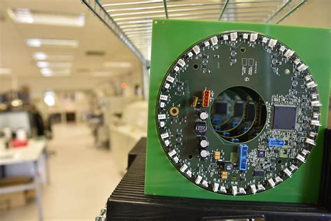
BGA (Ball Grid Array)
A package with a grid array of solder balls on the underside for high pin density. The balls are soldered directly to round pads on the PCB. BGAs can have hundreds of balls with pitches down to 0.3mm. X-ray inspection is usually needed.
CSP (Chip Scale Package)
Chip scale packages are very compact, with a package size only slightly larger than the die itself (within 1.2X). Includes FBGA, μBGA, and wafer-level CSP.
PoP (Package on Package)
PoP is a stacked packaging method where one component package (e.g. memory) is soldered on top of another (e.g. processor) to save board space in compact devices like smartphones.

SMT Design Guidelines
To ensure manufacturability and reliability, PCB designs for SMT assembly should follow some basic rules and guidelines:
-
Pad Size and Spacing – The footprint for each component, including the size, shape, and spacing of the pads, should match the dimensions specified in the datasheet or standard (e.g. IPC-7351B). The pad should be slightly larger than the component termination to allow for some placement tolerance.
-
Pad Finish – The surface finish on the component pads affects solderability. Hot Air Solder Leveling (HASL), Organic Solderability Preservative (OSP), Electroless Nickel Immersion Gold (ENIG) and Immersion Silver (IAg) are common finishes compatible with SMT. Each has pros and cons in terms of cost, shelf life, and durability.
-
Solder Mask – A solder mask layer on the PCB helps prevent solder bridging and protect the traces. The mask apertures should be slightly larger than the pads (typically 0.05mm) to avoid interfering with the solder joint. For fine-pitch components, a liquid photoimageable (LPI) mask with precise registration is needed.
-
Silkscreen – The silkscreen legend on the PCB should clearly indicate the component designators and polarity marks. The markings should not overlap pads and should leave space for the solder mask expansion. A white color is typical, but other colors like yellow or black may be used for contrast.
-
Placement Clearance – Adequate space should be left around each component for the placement nozzle to approach the part without colliding with adjacent components. Fine-pitch or fragile parts may need more clearance.
-
Thermal Design – Copper pours, thermal vias, and other heatsinking techniques should be used as needed to dissipate heat from power-hungry components. The thermal mass and conductivity of the PCB affects how quickly and evenly it heats and cools during reflow.
-
Panelization – Individual PCBs are often panelized into a larger array for more efficient assembly. Rails, tabs, or mousebites are used to hold the boards together. Fiducials on the panel aid in placement registration. V-score or tab-route breakaway features allow the individual boards to be separated after assembly.
-
Design For Test – Whenever possible, test points, vias, or pads should be provided for key signals and power rails to enable in-circuit testing and debug. Components should be placed to allow access for probes or inspection. Boundary scan and other DFT techniques should be leveraged.
By following SMT DFM (Design For Manufacturing) guidelines, PCB designers can help maximize assembly yields, minimize defects, and reduce manufacturing costs and turnaround time.

Advantages of SMT PCB Assembly
SMT PCB assembly offers many advantages over through-hole mounting:
-
Smaller Size – SMT components are much smaller than their through-hole counterparts, allowing for more compact PCB designs with higher component density. This is essential for modern consumer electronics like smartphones and wearables.
-
Lighter Weight – SMT boards are typically 1/3 to 1/2 the weight of equivalent through-hole boards due to the smaller components and elimination of leads and drilled holes. This is important for portable and aerospace applications.
-
Lower Cost – Despite the higher initial cost for setup and equipment, SMT is more economical than through-hole in volume production due to the automated assembly process, fewer drilling and finishing steps, and less material waste.
-
Faster Assembly – With high-speed pick and place machines and reflow ovens, SMT boards can be assembled much faster than through-hole boards, which require manual insertion and wave soldering. This higher throughput reduces labor costs.
-
Better Performance – SMT provides better mechanical and electrical performance than through-hole. The smaller lead lengths and closer spacing reduce stray inductance and capacitance for faster signal speeds. The lower mass and direct attachment to the board improve shock and vibration resistance.
-
Double-Sided Assembly – SMT allows components to be mounted on both sides of the PCB, effectively doubling the available area for components. Through-hole parts can only be mounted on one side.
-
Easier Automation – The standardized packaging and assembly process for SMT is well-suited for automation, with minimal human intervention required. This improves consistency and reliability.
-
Flexible Design – With the wide range of SMT package types and sizes available, PCBs can be designed with greater flexibility to optimize performance, cost, and manufacturability for the specific application.
While through-hole mounting is still used for certain components and applications, SMT has become the dominant PCB assembly technology for its clear benefits in size, cost, and performance.
Challenges of SMT PCB Assembly
Despite its many advantages, SMT PCB assembly does present some challenges compared to through-hole:
-
Component Handling – SMT components, especially chip passives, are very small and delicate, requiring specialized feeders, nozzles, and placement heads to handle properly without damage. The parts are sensitive to moisture, static, and thermal shock.
-
Solder Joint Defects – SMT solder joints are more prone to certain defects like poor wetting, voids, bridging, tombstoning, and head-in-pillow. These can be caused by issues with the solder paste, reflow profile, component placement, or board design.
-
Thermal Management – With higher component density and double-sided assembly, SMT boards can be more challenging to cool properly. Careful thermal design and heat sinking is needed to prevent overheating


Leave a Reply