Understanding the Basics of SMT PCB Assembly
Before diving into the instructions, it’s important to understand the fundamentals of SMT PCB assembly. SMT is a method of assembling electronic components directly onto the surface of a PCB, as opposed to through-hole technology where components are inserted into holes drilled in the board.
Advantages of SMT PCB Assembly
- Smaller component sizes
- Higher component density
- Improved electrical performance
- Reduced manufacturing costs
- Faster assembly process
Step 1: Prepare the PCB and Components
The first step in SMT PCB assembly is to prepare the PCB and components. This involves the following tasks:
-
PCB Cleaning: Clean the PCB surface to remove any contaminants or debris that may affect the assembly process. Use a specialized PCB cleaner or isopropyl alcohol to ensure a clean surface.
-
Solder Paste Stencil: Apply solder paste to the PCB using a stencil. The stencil is a thin metal sheet with apertures that correspond to the pads on the PCB. Place the stencil over the PCB and apply solder paste using a squeegee.
-
Component Placement: Organize the surface mount components according to the PCB layout. Ensure that the components are properly oriented and placed in the correct locations.

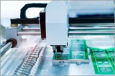
Step 2: Pick and Place Components
Once the PCB and components are prepared, the next step is to pick and place the components onto the PCB. This process can be done manually or using an automated pick and place machine.
Manual Pick and Place
For small-scale production or prototyping, manual pick and place is a viable option. Use tweezers or a vacuum pen to carefully place each component onto the corresponding pads on the PCB. Ensure proper alignment and orientation of the components.
Automated Pick and Place
For larger production runs, an automated pick and place machine is recommended. These machines use computer-controlled nozzles to pick up components from reels or trays and place them accurately on the PCB. The machine is programmed with the PCB layout and component specifications to ensure precise placement.

Step 3: Reflow Soldering
After the components are placed on the PCB, the next step is to perform reflow soldering. Reflow soldering is a process where the PCB assembly is heated to melt the solder paste and create a permanent bond between the components and the PCB.
Reflow Oven
A reflow oven is used for this process. The PCB assembly is placed on a conveyor belt and passes through the oven, which has a controlled temperature profile. The temperature profile typically includes the following stages:
-
Preheat: The PCB is gradually heated to a temperature below the melting point of the solder paste. This stage helps to evaporate any solvents and activate the flux in the solder paste.
-
Soak: The temperature is maintained for a specific duration to ensure even heating and to allow the components to settle onto the pads.
-
Reflow: The temperature is raised above the melting point of the solder paste, causing the solder to melt and form a connection between the components and the PCB pads.
-
Cooling: The PCB assembly is cooled down to solidify the solder joints.

Step 4: Inspection and Quality Control
After the reflow soldering process, it’s crucial to inspect the PCB assembly for any defects or issues. Visual inspection and automated optical inspection (AOI) are commonly used methods.
Visual Inspection
Visual inspection involves examining the PCB assembly under magnification to check for any visible defects such as:
- Misaligned components
- Solder bridges
- Insufficient or excessive solder
- Damaged components
Automated Optical Inspection (AOI)
AOI uses high-resolution cameras and image processing algorithms to automatically detect and identify defects on the PCB assembly. AOI systems can quickly scan the entire PCB and highlight any areas of concern for further review.
Step 5: Rework and Repair
If any defects or issues are identified during the inspection process, rework and repair may be necessary. This involves removing the defective component, cleaning the PCB pads, and resoldering a new component in its place.
Desoldering Techniques
To remove a defective component, various desoldering techniques can be used, such as:
- Desoldering braid: A copper braid that absorbs molten solder when heated.
- Desoldering pump: A manual or electric device that sucks up molten solder.
- Hot air rework station: A tool that uses a focused stream of hot air to melt solder and remove components.
Resoldering Process
After removing the defective component and cleaning the PCB pads, a new component is placed and soldered using a soldering iron or hot air rework station. Ensure proper alignment and solder joint quality during the resoldering process.
Step 6: Conformal Coating (Optional)
Conformal coating is an optional step in SMT PCB assembly that involves applying a protective layer over the PCB and components. This coating helps to protect the assembly from environmental factors such as moisture, dust, and corrosion.
Types of Conformal Coatings
There are several types of conformal coatings available, including:
- Acrylic
- Silicone
- Polyurethane
- Epoxy
The choice of conformal coating depends on the specific requirements of the application, such as the level of protection needed, operating environment, and compatibility with the components.
Application Methods
Conformal coating can be applied using various methods, such as:
- Brush coating
- Spray coating
- Dip coating
- Selective coating (using a dispensing system)
Ensure that the coating is applied evenly and covers all critical areas of the PCB assembly.
Step 7: Final Testing and Functional Verification
Before considering the SMT PCB assembly complete, it’s essential to perform final testing and functional verification. This step ensures that the assembled PCB functions as intended and meets the specified requirements.
In-Circuit Testing (ICT)
In-circuit testing involves using a bed-of-nails fixture to make electrical contact with specific points on the PCB. The fixture is connected to a test system that applies stimuli and measures the response to verify the functionality of individual components and circuits.
Functional Testing
Functional testing involves powering up the PCB assembly and testing its overall functionality. This may include running software tests, checking input/output signals, and verifying the performance of the device under various conditions.
Step 8: Packaging and Shipping
Once the SMT PCB assembly has passed the final testing and functional verification, it’s ready for packaging and shipping. Proper packaging ensures that the assembled PCBs are protected during transportation and reach the customer in good condition.
Packaging Materials
Use appropriate packaging materials based on the size, quantity, and fragility of the PCB assemblies. Common packaging materials include:
- Anti-static bags
- Bubble wrap
- Foam inserts
- Corrugated boxes
Labeling and Documentation
Include necessary labels and documentation with the packaged PCB assemblies, such as:
- Product identification labels
- Quantity and batch information
- Quality control certificates
- Shipping documents
Step 9: Continuous Improvement and Process Optimization
To maintain the quality and efficiency of your SMT PCB assembly process, it’s important to continuously monitor, analyze, and optimize the process. This involves:
-
Collecting and analyzing data: Gather data on key metrics such as throughput, defect rates, and cycle times. Use this data to identify areas for improvement.
-
Implementing process improvements: Based on the data analysis, implement changes to optimize the assembly process. This may include adjusting machine settings, improving operator training, or streamlining material handling.
-
Monitoring and reviewing: Continuously monitor the impact of the implemented improvements and make further adjustments as needed. Regularly review the assembly process to identify new opportunities for optimization.
By following these 9 detailed instructions, you can successfully complete your SMT PCB assembly and ensure high-quality, reliable electronic devices.
Frequently Asked Questions (FAQ)
1. What is the difference between SMT and through-hole PCB assembly?
SMT (Surface Mount Technology) involves placing components directly onto the surface of the PCB, while through-hole assembly requires inserting component leads through holes drilled in the PCB. SMT allows for smaller component sizes, higher density, and faster assembly compared to through-hole.
2. Can I mix SMT and through-hole components on the same PCB?
Yes, it is possible to have a mix of SMT and through-hole components on the same PCB. This is known as a hybrid assembly. However, it’s important to consider the assembly sequence and ensure compatibility between the two technologies.
3. What is the purpose of solder paste in SMT PCB assembly?
Solder paste is a mixture of tiny solder particles and flux. It is applied to the PCB pads before component placement. During the reflow soldering process, the solder paste melts and forms a permanent electrical and mechanical connection between the components and the PCB.
4. How do I choose the right solder paste for my SMT PCB assembly?
When selecting solder paste, consider factors such as the alloy composition (e.g., lead-free or leaded), particle size, and flux type (e.g., rosin-based, water-soluble, or no-clean). The choice depends on the specific requirements of your application, such as the component sizes, reflow profile, and environmental considerations.
5. What are some common defects in SMT PCB assembly, and how can they be prevented?
Common defects in SMT PCB assembly include solder bridges, insufficient or excessive solder, tombstoning (component standing up on one end), and component misalignment. These defects can be prevented by ensuring proper solder paste application, accurate component placement, optimized reflow profile, and regular maintenance of the assembly equipment.
| Defect | Description | Prevention |
|---|---|---|
| Solder Bridge | Unintended connection between two or more pads due to excessive solder | Proper solder paste application, optimized reflow profile |
| Insufficient Solder | Weak or incomplete solder joint due to insufficient solder paste | Proper solder paste application, stencil design |
| Excessive Solder | Solder joint with too much solder, may cause short circuits | Proper solder paste application, optimized reflow profile |
| Tombstoning | Component standing up on one end due to uneven heating or surface tension | Balanced pad design, proper component placement, optimized reflow profile |
| Component Misalignment | Component not placed accurately on the pads | Accurate pick and place, regular maintenance of assembly equipment |
By understanding these common defects and implementing the appropriate prevention measures, you can minimize their occurrence and improve the overall quality of your SMT PCB assembly.


Leave a Reply