Introduction
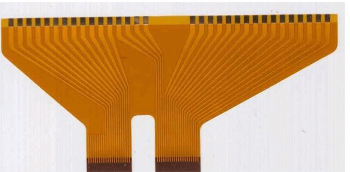
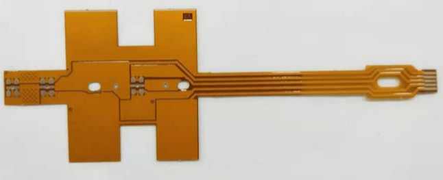
Flexible printed circuit boards (Flex PCBs) have become an increasingly popular solution for connecting electronic components in situations where rigid boards are impractical. With their ability to bend and flex, these circuits can fit into tight spaces and move within an electronic device. Designing flex PCBs requires specialized knowledge to account for their unique mechanical properties during layout and fabrication. Altium Designer provides flex PCB designers with specific tools to create robust and reliable flexible circuits. This article will explore how Altium enables flex PCB design, including handling flex-rigid combinations, autorouting, and generating fabrication outputs.
Benefits of Flexible PCBs
Flexible PCBs provide several advantages over traditional rigid boards:
- Fit into tight spaces – Can fold and bend to fit into small devices. Useful when space constraints exist.
- Move within devices – Dynamic flexing allows movement and articulation in products.
- Lower weight – Thinner and lighter than rigid boards. Important for portable devices.
- Reliability – Can handle repeated bending without damage. Withstands vibration and impact.
- Lower cost – Requires less material than rigid PCBs. Simpler fabrication process.
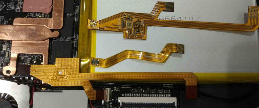
Flex PCBs integrate well with rigid PCBs through flex-rigid combinations. This allows designers to optimize the layout using both flexible and rigid sections of circuitry.
Design Considerations for Flex PCBs
Although flexible PCBs provide many benefits, they also come with some unique design considerations:
- Bending radius – Avoid too tight of bends that could damage copper traces.
- Layer stackup – Ensure adequate flexible substrate layers and adhesive choices.
- Component placement – Position parts to avoid areas of maximum bend stress.
- Copper relief patterns – Relieve copper near bend areas to prevent cracks.
- Stiffener integration – Add rigid sections or stiffeners to prevent flexing damage.
Paying attention to these areas will result in a flex PCB that meets circuit functionality and reliability requirements.
Flexible PCB Layout in Altium Designer
Altium Designer incorporates specialized features and options to facilitate flex PCB design while addressing the key considerations.
Defining Flex Layer Stacks
The first step is to define the layer stack for the flex PCB substrate materials. This is done in the Layer Stack Manager. Some key settings include:
- Choosing flex substrate layers such as polyimide
- Adding cover layers like acrylic adhesive
- Assigning dielectric constants and thicknesses
- Enabling automatic teardrops on pads
Flexible layers can be combined with rigid layers for flex-rigid boards. Rigid-Flex Settings define the regions.
Optimized Drawing Tools
The PCB editor includes modes and settings for efficient flex PCB layout:
- Flex mode display – Highlights rigid/flex boundary segments
- Preferred direction routing – Follows flex layer bending axis
- Smoothed routing – Reduces angular routing on flex layers
- Arc and bend routing – Controls routing along bend guidelines
Managing Bends and Copper Relief
To handle bending requirements, designers can:
- Define minimum bend radii rules
- Insert board fold lines and view dynamic bend radius arcs
- Utilize teardrop pads on flex layers
- Add crosshatch copper relief patterns
Autorouting Flex PCBs
The autorouter automatically handles flex PCB constraints like:
- Respecting flex layer preferred routing directions
- Maintaining clearance from board folds and edges
- Honoring minimum bend radius rules
- Including arc and smoothed segments where needed
Fabrication Outputs and Drawings
Altium generates industry-standard manufacturing outputs from the flex design while accounting for things like:
- Layer stacks tailored to flex PCB fabrication
- Routed flex layer bending profiles
- Drill drawings with slots for flex board bends
- 3D PDFs with integrated board folds and folds
These specialized outputs ensure manufacturers have the information needed to produce the flex PCB correctly.
Additional Functionality
Other helpful features in Altium for flex PCB design include:
- Flex-rigid signal isolation rules
- Split power planes across bends
- Cross-probing between 2D and 3D views
- Interactive 3D flex PCB views
- Automatic panelization of flex circuits
Layout Best Practices for Flex PCBs in Altium
Following layout best practices in Altium Designer will help achieve successful flex PCB designs:
- Minimize component placement near board edges vulnerable to bending
- Orient components to avoid tombstoning during flexing
- Understand dynamic flexing effects with rigid-flex simulations
- Use dedicated flex layers for interconnects spanning bends
- Allow adequate clearances between conductors at bent sections
- Minimize rigid sections on outer bends of the flex PCB
Applying these guidelines and others specific to each design will result in flex PCB layouts that meet reliability requirements.
Flex PCB Layout Comparison
Here is a comparison of a poorly designed flex PCB layout versus a good layout in Altium:
| Poor Layout | Good Layout |
|---|---|
| – Components placed near bends | – Components away from bends |
| – No copper relief | – Copper relief included |
| – Rigid sections on outer bends | – Rigid sections on inner bends |
| – No stiffeners used | – Stiffeners added |
| – Tight bend radii | – Bend radius rules followed |
Simulating Flex PCBs
To verify flex PCB designs, Altium includes 3D simulation capabilities. Some analysis features include:
- Viewing dynamic flexing behavior
- Detecting collisions as flexing occurs
- Identifying component stresses across full range of motion
- Optimizing placement to reduce stresses
- Predicting fatigue life based on flex cycles
- Finding resonant vibration frequencies
These types of simulations reduce reliance on physical prototypes, saving cost and time.
Here is an example simulation in Altium showing a flex PCB bending:<img src=”images/flex_simulation.gif” width=”400″>
Manufacturing Flexible PCBs
When the design is complete, fabricating flex PCBs requires special manufacturing considerations:
| Process | Description |
|---|---|
| Etching | Use cupric chloride etching optimized for flex circuits |
| Solder mask | Liquid photoimageable solder mask withstands flexing |
| Hot air soldering | Preferred technique to avoid mechanical stress |
| Electrical testing | Fixtures must securely hold flex PCBs during probing |
| Assembly | Adhesives and methods selected to allow dynamic movement |
| Encapsulation | Conformal coating protects against wear and moisture |
Working closely with the board manufacturer ensures these processes are handled properly.
Applications of Flexible PCBs
Some common applications making use of flex PCB technology include:
- Wearable electronics
- Medical devices
- Robotics
- Automotive electronics
- Consumer gadgets
- Industrial equipment
- Aerospace systems
As demands grow for smaller, lighter, and more reliable electronics, flex PCBs will continue increasing in popularity moving forward.
Flex PCBs with Altium – FAQ
What are some key advantages of flexible PCBs?
Some major advantages are their ability to:
- Fit into tight spaces where rigid PCBs won’t work
- Flex and move dynamically within devices
- Withstand vibration and impacts without damage
- Achieve lighter weight and lower cost
What are some best practices to follow when laying out flex PCBs?
Some layout best practices include:
- Avoid components near bend areas
- Use rigid sections carefully on inner bends
- Include copper relief patterns
- Maintain adequate clearance at flex points
- Follow minimum bend radius rules
- Simulate dynamic flexing effects
How does Altium make designing flex PCBs easier?
Altium has specialized features for flex circuits like:
- Layer stacks for flex materials
- Auto routing tailored for flex layers
- Drawing tools optimized for flex bends
- Integrated rigid-flex settings
- 3D simulations of flexing behavior
- Manufacturing outputs targeting flex fabrication
What type of analysis is important when evaluating flex PCBs?
Important analyses include:
- Visualizing dynamic bend motions
- Finding failures during range of motion
- Detecting component stresses and fatigue life
- Optimizing placement to reduce stress
- Predicting vibration modes and frequencies
What are some applications that benefit from using flex PCBs?
Common applications include:
- Wearable devices
- Medical equipment
- Robotics joints
- Consumer gadgets
- Automotive electronics
- Aerospace systems
Flex PCBs fit well when space is constrained, movement is required, or durability is important.


Leave a Reply