Introduction to PCB Stencils
PCB stencils are essential tools in the Electronic Manufacturing process, allowing for precise and efficient application of solder paste onto printed circuit boards (PCBs). These stencils are typically made from durable materials such as stainless steel or polyimide and feature apertures that correspond to the pads on the PCB. By using a PCB stencil, manufacturers can ensure consistent and accurate solder paste deposition, which is crucial for achieving reliable solder joints and overall product quality.
The Role of PCB Stencils in Electronic Manufacturing
In the fast-paced world of electronic manufacturing, PCB stencils play a vital role in streamlining the assembly process and ensuring the production of high-quality PCBs. Some key benefits of using PCB stencils include:
- Improved accuracy: PCB stencils enable precise control over the amount and placement of solder paste on the PCB pads, reducing the risk of defects such as bridging or insufficient solder.
- Increased efficiency: By automating the solder paste application process, PCB stencils help to speed up production and reduce manual labor, ultimately leading to cost savings.
- Enhanced consistency: PCB stencils ensure that solder paste is applied uniformly across the entire PCB, resulting in consistent solder joint quality and improved product reliability.
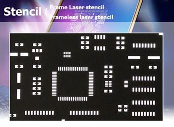
Types of PCB Stencils
There are several types of PCB stencils available, each with its own unique characteristics and advantages:
- Stainless steel stencils: These stencils are known for their durability, precision, and long lifespan. They are ideal for high-volume production and can withstand repeated use without deformation.
- Polyimide stencils: Made from a flexible polymer material, polyimide stencils are well-suited for applications that require conformity to uneven surfaces or tight tolerances. They are also more cost-effective than stainless steel stencils.
- Electroformed stencils: Electroformed stencils are created using a process that involves depositing metal onto a master pattern. They offer excellent detail resolution and are suitable for fine-pitch applications.
- Laser-Cut Stencils: These stencils are manufactured using high-precision laser cutting technology, allowing for intricate designs and quick turnaround times.
Choosing the Right PCB Stencil
Factors to Consider When Selecting a PCB Stencil
When choosing a PCB stencil for your electronic manufacturing needs, there are several key factors to consider:
- Material: As mentioned earlier, PCB stencils can be made from various materials, such as stainless steel or polyimide. Consider the specific requirements of your application, such as durability, flexibility, and cost, when selecting the appropriate material.
- Aperture size and shape: The size and shape of the apertures in the PCB stencil will determine the amount and distribution of solder paste on the PCB pads. Ensure that the aperture design is optimized for your specific component types and sizes.
- Thickness: PCB stencil thickness typically ranges from 0.1 mm to 0.2 mm (4 to 8 mils). Thicker stencils are generally used for larger components or higher solder paste volumes, while thinner stencils are suitable for finer pitch components.
- Surface finish: The surface finish of the PCB stencil can impact the release characteristics of the solder paste. Common surface finishes include electropolishing, nano-coating, and laser-cutting. Choose a surface finish that promotes clean, consistent solder paste release.
PCB Stencil Design Considerations
To ensure optimal performance and quality, it is essential to carefully design your PCB stencil. Some key design considerations include:
- Aperture size and shape: As mentioned earlier, the size and shape of the apertures in the PCB stencil will determine the amount and distribution of solder paste on the PCB pads. Aperture sizes should be carefully calculated based on the pad dimensions, component types, and desired solder paste volume.
- Stencil thickness: The thickness of the PCB stencil should be selected based on the specific requirements of your application. Thicker stencils are generally used for larger components or higher solder paste volumes, while thinner stencils are suitable for finer pitch components.
- Fiducial marks: Fiducial marks are reference points on the PCB stencil that help to align the stencil with the PCB during the solder paste printing process. Ensure that your stencil design includes appropriate fiducial marks for accurate alignment.
- Escape routing: In some cases, it may be necessary to incorporate escape routing into your PCB stencil design to allow for proper solder paste deposition on closely spaced pads. This involves creating channels or openings in the stencil to allow solder paste to flow between adjacent pads.
PCB Stencil Manufacturers and Service Providers
When sourcing PCB stencils for your electronic manufacturing needs, it is important to choose a reputable manufacturer or service provider. Some factors to consider when selecting a PCB stencil supplier include:
- Experience and expertise: Look for a supplier with a proven track record of producing high-quality PCB stencils and a deep understanding of the electronic manufacturing process.
- Manufacturing capabilities: Ensure that the supplier has the necessary equipment and technology to produce PCB stencils that meet your specific requirements, such as laser cutting or electroforming.
- Quality control: Choose a supplier that adheres to strict quality control standards and conducts thorough inspections to ensure that each PCB stencil meets the highest standards of accuracy and consistency.
- Customer support: Look for a supplier that offers excellent customer support and is responsive to your needs and concerns throughout the PCB stencil purchasing process.

Advanced PCB Stencil Technologies
Step Stencils
Step stencils, also known as multi-level stencils, are an advanced PCB stencil technology that allows for the deposition of different solder paste volumes on different areas of the PCB. This is achieved by creating a stencil with multiple levels or steps, each with its own aperture size and thickness. Step stencils are particularly useful for PCBs with components of varying sizes and heights, as they enable the precise control of solder paste volume for each component type.
Solder Preforms
Solder preforms are pre-shaped pieces of solder that can be used in conjunction with PCB stencils to improve solder joint quality and reliability. These preforms are typically placed on the PCB pads prior to solder paste printing and are designed to melt and flow during the reflow process, creating a strong and consistent solder joint. Solder preforms are available in various shapes and sizes and can be customized to suit specific application requirements.
3D Printed Stencils
3D printed stencils are an emerging technology that offers several advantages over traditional PCB stencils. By using additive manufacturing techniques, 3D printed stencils can be produced quickly and cost-effectively, with minimal waste material. Additionally, 3D printing allows for the creation of complex stencil geometries and features that may be difficult or impossible to achieve with traditional manufacturing methods. However, the long-term durability and performance of 3D printed stencils are still being evaluated, and they may not be suitable for all applications.

PCB Stencil Maintenance and Cleaning
To ensure consistent performance and longevity, it is essential to properly maintain and clean your PCB stencils. Some key maintenance and cleaning considerations include:
- Regular inspection: Regularly inspect your PCB stencils for signs of wear, damage, or contamination. Look for issues such as bent or warped stencils, clogged apertures, or excessive solder paste buildup.
- Cleaning: Clean your PCB stencils regularly to remove solder paste residue and prevent contamination. Use appropriate cleaning solutions and methods, such as ultrasonic cleaning or manual wiping, depending on the type of stencil and the nature of the contamination.
- Storage: Store your PCB stencils in a clean, dry environment to prevent damage and contamination. Consider using stencil storage racks or containers to keep your stencils organized and protected.
- Handling: Handle your PCB stencils with care to avoid damage or deformation. Use gloves or other protective equipment to minimize the risk of contamination and ensure that the stencils are properly supported during handling and transport.
PCB Stencil Cleaning Methods
There are several methods for cleaning PCB stencils, each with its own advantages and considerations:
- Manual cleaning: Manual cleaning involves wiping the stencil with a lint-free cloth or paper towel soaked in a cleaning solution. This method is suitable for light contamination and is relatively quick and easy to perform.
- Ultrasonic cleaning: Ultrasonic cleaning uses high-frequency sound waves to agitate a cleaning solution, creating tiny bubbles that help to remove solder paste residue and contamination from the stencil surface and apertures. This method is more effective than manual cleaning and is suitable for removing heavy contamination.
- Spray cleaning: Spray cleaning involves using a pressurized spray of cleaning solution to remove solder paste residue and contamination from the stencil surface. This method is quick and efficient but may not be as effective as ultrasonic cleaning for removing heavy contamination.
- Automated cleaning: Automated cleaning systems use a combination of brushes, rollers, and cleaning solutions to clean PCB stencils in a controlled and consistent manner. These systems are ideal for high-volume production environments and can significantly reduce the time and labor required for stencil cleaning.
| Cleaning Method | Advantages | Disadvantages |
|---|---|---|
| Manual Cleaning | – Quick and easy – Low cost – Suitable for light contamination |
– Labor-intensive – May not remove heavy contamination – Risk of stencil damage |
| Ultrasonic Cleaning | – Effective for heavy contamination – Thorough cleaning of apertures – Automated process |
– Higher cost than manual cleaning – Requires specialized equipment – May not be suitable for delicate stencils |
| Spray Cleaning | – Quick and efficient – Suitable for moderate contamination – Less labor-intensive than manual cleaning |
– May not remove heavy contamination – Risk of stencil damage from high-pressure spray – Requires specialized equipment |
| Automated Cleaning | – Consistent and controlled cleaning – High-volume capability – Reduced labor requirements |
– High initial cost – Complex setup and maintenance – May not be suitable for all stencil types |

Frequently Asked Questions (FAQ)
- What is the difference between a PCB stencil and a solder paste mask?
-
A PCB stencil is a thin sheet of metal or polymer with apertures that correspond to the pads on a PCB, used for applying solder paste. A solder paste mask, on the other hand, is a layer of material applied directly to the PCB to prevent solder paste from adhering to non-pad areas.
-
How often should I clean my PCB stencils?
-
The frequency of PCB stencil cleaning depends on factors such as the type of solder paste used, the volume of production, and the environment. As a general rule, stencils should be cleaned whenever there is visible solder paste residue or contamination, or when print quality begins to deteriorate.
-
Can I reuse my PCB stencils?
-
Yes, PCB stencils can be reused multiple times with proper cleaning and maintenance. However, the lifespan of a stencil will depend on factors such as the material, thickness, and handling. Regularly inspect your stencils for signs of wear or damage and replace them as needed.
-
What is the optimal PCB stencil thickness for my application?
-
The optimal PCB stencil thickness depends on factors such as the component types, pad sizes, and desired solder paste volume. As a general guideline, stencils with a thickness of 0.1 mm to 0.15 mm (4 to 6 mils) are suitable for most standard SMT applications, while thicker stencils (0.15 mm to 0.2 mm, or 6 to 8 mils) may be needed for larger components or higher solder paste volumes.
-
How do I choose the right PCB stencil aperture size and shape?
- The size and shape of PCB stencil apertures should be based on the pad dimensions, component types, and desired solder paste volume. As a starting point, apertures are typically designed to be slightly larger than the pad size (10% to 20%) to allow for adequate solder paste deposition. The exact aperture dimensions and shapes may need to be optimized through testing and iteration to achieve the desired solder paste print quality.
Conclusion
PCB stencils are critical tools in the electronic manufacturing process, enabling the precise and efficient application of solder paste onto PCBs. By understanding the types of PCB stencils available, the factors to consider when selecting and designing stencils, and the importance of proper maintenance and cleaning, manufacturers can optimize their solder paste printing process and ensure the production of high-quality, reliable electronic products.
As PCB designs continue to evolve and become more complex, advanced PCB stencil technologies such as step stencils, solder preforms, and 3D printed stencils offer new opportunities for improving solder joint quality and reliability. By staying up-to-date with these emerging technologies and best practices, manufacturers can remain competitive and meet the ever-increasing demands of the electronics industry.
Ultimately, the successful implementation of PCB stencils in the electronic manufacturing process requires a combination of careful design, material selection, maintenance, and collaboration with experienced stencil manufacturers and service providers. By taking a comprehensive approach to PCB stencil management, manufacturers can unlock the full potential of these essential tools and drive innovation, efficiency, and quality in their electronic products.


Leave a Reply