What is a PCB Stencil?
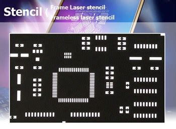
A PCB stencil is a thin sheet of stainless steel or polyimide film with a pattern of apertures that match the pads on a printed circuit board (PCB). It is used to apply solder paste onto the PCB pads during the surface mount assembly process. The stencil ensures that the correct amount of solder paste is deposited on each pad, which is crucial for achieving reliable solder joints.
PCB Stencils are an essential tool in modern electronics manufacturing. They enable the precise and consistent application of solder paste, which is necessary for high-quality surface mount assembly. Without a stencil, it would be extremely difficult and time-consuming to apply solder paste manually, and the results would be far less consistent.
Types of PCB Stencils
There are two main types of PCB stencils: stainless steel and polyimide film.
Stainless Steel Stencils
Stainless steel stencils are the most common type of PCB stencil. They are made from a thin sheet of stainless steel, typically 0.1 to 0.2 mm thick, with laser-cut apertures that match the pads on the PCB. Stainless steel stencils are durable, reusable, and can withstand the high temperatures of the reflow soldering process.
| Thickness (mm) | Typical Applications |
|---|---|
| 0.1 | Fine pitch components (0.3 mm and below) |
| 0.15 | Standard SMD components |
| 0.2 | Large components, high volume production |
Polyimide Film Stencils
Polyimide film stencils, also known as polymer stencils or solder paste stencils, are made from a thin sheet of polyimide film with laser-cut apertures. They are typically 0.05 to 0.1 mm thick and are more flexible than stainless steel stencils. Polyimide film stencils are often used for prototyping or low-volume production, as they are less expensive and easier to manufacture than stainless steel stencils.
| Thickness (mm) | Typical Applications |
|---|---|
| 0.05 | Ultra-fine pitch components (0.2 mm and below) |
| 0.08 | Fine pitch components (0.3 mm and below) |
| 0.1 | Standard SMD components, prototyping |

How to Make a PCB Stencil
Making a PCB stencil involves several steps, including designing the stencil, choosing the material, and cutting the apertures.
Step 1: Design the Stencil
The first step in making a PCB stencil is to design the stencil based on the PCB layout. This involves creating a stencil file that contains the aperture data for each pad on the PCB. The stencil file is typically created using a CAD software package, such as Altium Designer or KiCad.
When designing the stencil, it is important to consider factors such as the size and shape of the pads, the spacing between pads, and the thickness of the stencil material. The aperture size and shape should be optimized for the specific solder paste and components being used.
Step 2: Choose the Stencil Material
The next step is to choose the material for the stencil. As mentioned earlier, the two main options are stainless steel and polyimide film. The choice of material depends on factors such as the required durability, the complexity of the PCB layout, and the production volume.
Stainless steel is the most common choice for high-volume production, as it is durable and can withstand multiple print cycles. Polyimide film is often used for prototyping or low-volume production, as it is less expensive and easier to manufacture.
Step 3: Cut the Apertures
Once the stencil design is complete and the material has been chosen, the next step is to cut the apertures in the stencil. This is typically done using a laser cutting machine, which uses a high-powered laser to precisely cut the apertures in the stencil material.
The laser cutting process involves placing the stencil material in the machine and aligning it with the stencil file. The machine then uses the laser to cut the apertures according to the stencil file. The cutting process is highly automated and can produce stencils with very fine details and tight tolerances.
After the apertures have been cut, the stencil is cleaned and inspected for any defects or irregularities. Any necessary adjustments or repairs are made before the stencil is ready for use.

Factors to Consider When Making a PCB Stencil
When making a PCB stencil, there are several factors to consider to ensure that the stencil performs optimally and produces high-quality solder joints.
Aperture Size and Shape
The size and shape of the apertures in the stencil are critical factors in determining the amount and distribution of solder paste on the PCB pads. The aperture size should be slightly larger than the pad size to allow for some over printing, but not so large that it causes bridging or solder beads.
The aperture shape should also be optimized for the specific solder paste and components being used. Common aperture shapes include square, circular, and home plate.
Stencil Thickness
The thickness of the stencil material affects the amount of solder paste deposited on the pads. Thicker stencils deposit more paste, while thinner stencils deposit less. The optimal thickness depends on factors such as the size and pitch of the components, the viscosity of the solder paste, and the print speed and pressure.
| Component Pitch | Recommended Stencil Thickness |
|---|---|
| 0.3 mm and below | 0.1 mm |
| 0.4 mm to 0.5 mm | 0.15 mm |
| 0.6 mm and above | 0.2 mm |
Stencil Material
The choice of stencil material affects the durability, print quality, and cost of the stencil. Stainless steel is the most common choice for high-volume production, as it is durable and can withstand multiple print cycles. Polyimide film is often used for prototyping or low-volume production, as it is less expensive and easier to manufacture.
Stencil Frame
The stencil frame holds the stencil in place during the printing process and ensures that it remains flat and stable. The frame should be compatible with the printing equipment and should provide adequate support and tension to the stencil material.

PCB Stencil FAQs
- What is the difference between a PCB stencil and a solder paste screen?
-
A PCB stencil is a thin sheet of metal or polyimide film with apertures that match the pads on the PCB, while a solder paste screen is a woven mesh screen with a similar pattern of apertures. Stencils are more commonly used in modern electronics manufacturing due to their higher precision and durability.
-
Can I reuse a PCB stencil?
-
Yes, stencils can be cleaned and reused multiple times, especially if they are made of stainless steel. However, the stencil should be inspected for wear and damage after each use and replaced if necessary to ensure consistent print quality.
-
How do I clean a PCB stencil?
-
PCB stencils can be cleaned using a variety of methods, including manual cleaning with solvents and wipers, ultrasonic cleaning, and automated stencil cleaning systems. The choice of cleaning method depends on the type of solder paste and flux used, as well as the level of contamination on the stencil.
-
What is the typical lifespan of a PCB stencil?
-
The lifespan of a PCB stencil depends on various factors, such as the material, thickness, and usage frequency. Stainless steel stencils can typically last for thousands of print cycles, while polyimide film stencils may only last for a few hundred cycles.
-
Can I make my own PCB stencil at home?
- While it is possible to make a basic PCB stencil at home using materials such as vinyl or mylar sheets and a craft cutter, the results are likely to be less precise and consistent than professionally manufactured stencils. For best results, it is recommended to use a professional stencil manufacturing service.
Conclusion
PCB stencils are an essential tool in modern electronics manufacturing, enabling the precise and consistent application of solder paste for surface mount assembly. Making a PCB stencil involves designing the stencil based on the PCB layout, choosing the appropriate material and thickness, and cutting the apertures using a laser machine.
When making a PCB stencil, it is important to consider factors such as aperture size and shape, stencil thickness, material, and frame compatibility to ensure optimal performance and print quality. By understanding these factors and following best practices for stencil design and manufacturing, you can produce high-quality PCB stencils that will help you achieve reliable and efficient surface mount assembly.


Leave a Reply