Introduction to PCB Stencils
PCB stencils are an essential tool in the fabrication of printed circuit boards (PCBs). They are used to apply solder paste onto the PCB pads, ensuring precise and consistent solder paste deposits. The accuracy of solder paste application is crucial for the proper functioning and reliability of the assembled PCB.
What are PCB Stencils?
PCB stencils are thin metal sheets, typically made of stainless steel or nickel, with laser-cut apertures that correspond to the solder pad locations on a PCB. The thickness of the stencil determines the amount of solder paste deposited on the pads. Stencils are designed using CAD software and are manufactured using high-precision laser cutting machines.
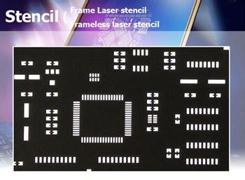
Types of PCB Stencils
There are two main types of PCB stencils:
-
Framed Stencils: These stencils are mounted on a rigid frame, providing stability and ease of handling. Framed stencils are suitable for high-volume production and automated assembly processes.
-
Frameless Stencils: These stencils are not mounted on a frame and are more flexible. Frameless stencils are often used for prototyping, low-volume production, and manual assembly processes.
The Role of PCB Stencils in the PCB Assembly Process
PCB stencils play a crucial role in the surface mount technology (SMT) assembly process. The SMT process involves placing surface mount components onto the PCB pads and soldering them in place. The solder paste application is the first step in this process, and it is where PCB stencils come into play.
Solder Paste Application
The solder paste application process using PCB stencils involves the following steps:
-
Stencil Alignment: The PCB stencil is aligned with the PCB using fiducial marks or dedicated alignment systems. Proper alignment ensures that the solder paste is deposited accurately on the pads.
-
Solder Paste Dispensing: Solder paste is placed on the stencil and spread across the surface using a squeegee. The squeegee forces the solder paste through the apertures and onto the PCB pads.
-
Stencil Removal: After the solder paste is applied, the stencil is carefully removed, leaving precisely deposited solder paste on the PCB pads.
Benefits of Using PCB Stencils
Using PCB stencils for solder paste application offers several benefits:
-
Precision: PCB stencils ensure accurate and consistent solder paste deposits on the PCB pads. This precision is essential for achieving reliable solder joints and preventing defects such as bridging or insufficient solder.
-
Efficiency: Stencil printing is a fast and efficient method for applying solder paste, especially in high-volume production. It allows for the simultaneous application of solder paste on multiple pads, reducing the overall assembly time.
-
Repeatability: PCB stencils provide consistent results across multiple PCBs, ensuring uniformity in the assembly process. This repeatability is crucial for maintaining product quality and reducing manufacturing errors.

Stencil Design Considerations
Proper stencil design is essential for achieving optimal solder paste application. Several factors need to be considered when designing PCB stencils:
Aperture Size and Shape
The size and shape of the stencil apertures determine the amount and profile of the solder paste deposited on the pads. The aperture dimensions should be carefully calculated based on the pad size, component pitch, and solder paste properties. Common aperture shapes include square, rectangular, and circular.
Stencil Thickness
The thickness of the stencil determines the volume of solder paste deposited on the pads. Thicker stencils deposit more solder paste, while thinner stencils deposit less. The optimal stencil thickness depends on the component size, pad dimensions, and solder paste characteristics. Typical stencil thicknesses range from 0.1 mm to 0.2 mm.
Aperture Walls
The walls of the stencil apertures should be designed to facilitate smooth solder paste release. Tapered walls or rounded corners can help prevent solder paste from sticking to the stencil and ensure clean paste deposits on the pads.
Stencil Material
The choice of stencil material depends on factors such as durability, cost, and compatibility with the solder paste. Stainless steel is the most common material for PCB stencils due to its strength, stability, and resistance to wear. Nickel stencils are also used in some applications for their non-stick properties and improved paste release.

Stencil Maintenance and Cleaning
Proper maintenance and cleaning of PCB stencils are essential for ensuring consistent solder paste application and preventing defects. Regular cleaning helps remove solder paste residue, prevents clogging of apertures, and extends the life of the stencil.
Cleaning Methods
There are several methods for cleaning PCB stencils:
-
Manual Cleaning: This involves using solvents and wiping the stencil with a lint-free cloth or brush. Manual cleaning is suitable for small-scale production and quick cleaning between prints.
-
Ultrasonic Cleaning: Ultrasonic cleaners use high-frequency sound waves to agitate a cleaning solution, effectively removing solder paste residue from the stencil. This method is more thorough and efficient than manual cleaning.
-
Automated Cleaning: Automated stencil cleaning systems use a combination of solvents, brushes, and air knives to clean the stencil. These systems are designed for high-volume production and provide consistent and reliable cleaning results.
Cleaning Frequency
The frequency of stencil cleaning depends on factors such as the solder paste type, production volume, and environmental conditions. In general, stencils should be cleaned:
- After every print cycle in high-volume production
- After a certain number of prints in low-volume production
- When there are visible signs of solder paste buildup or contamination
Regular inspection of the stencil can help determine the appropriate cleaning frequency and prevent defects caused by clogged apertures or solder paste residue.

Common Stencil-Related Defects and Troubleshooting
Despite the benefits of using PCB stencils, various defects can occur during the solder paste application process. Identifying and troubleshooting these defects is crucial for maintaining the quality of the assembled PCBs.
Solder Paste Bridging
Solder paste bridging occurs when excess solder paste connects adjacent pads, creating short circuits. This defect can be caused by:
- Overprinting (applying too much solder paste)
- Incorrect stencil aperture dimensions
- Misalignment between the stencil and PCB
To prevent bridging, ensure proper stencil design, alignment, and solder paste volume control.
Insufficient Solder Paste
Insufficient solder paste occurs when not enough paste is deposited on the pads, resulting in weak or open solder joints. This defect can be caused by:
- Underprinting (applying too little solder paste)
- Clogged stencil apertures
- Incorrect stencil thickness
To prevent insufficient solder paste, ensure proper stencil design, regular cleaning, and adequate solder paste volume.
Solder Paste Smearing
Solder paste smearing occurs when solder paste is dragged across the PCB surface during stencil removal, creating a messy appearance and potential short circuits. This defect can be caused by:
- Incorrect stencil removal technique
- Excessive solder paste volume
- Improper stencil cleaning
To prevent smearing, use proper stencil removal techniques, control solder paste volume, and maintain a clean stencil.
Frequently Asked Questions (FAQ)
-
What is the recommended stencil thickness for SMT components?
The recommended stencil thickness for SMT components depends on the component size and pitch. A general guideline is to use a stencil thickness that is 80% to 90% of the component lead height. For example, for components with a lead height of 0.5 mm, a stencil thickness of 0.4 mm to 0.45 mm is recommended. -
How often should PCB stencils be replaced?
The lifespan of a PCB stencil depends on factors such as usage, cleaning frequency, and storage conditions. In general, stencils should be replaced when there are visible signs of wear, damage, or contamination that cannot be removed by cleaning. Regular inspection of the stencil can help determine when replacement is necessary. -
Can PCB stencils be reused?
Yes, PCB stencils can be reused multiple times with proper cleaning and maintenance. However, the number of reuses depends on the stencil material, cleaning effectiveness, and storage conditions. It is important to inspect the stencil regularly for any signs of damage or wear that may affect its performance. -
What are the most common materials used for PCB stencils?
The most common materials used for PCB stencils are stainless steel and nickel. Stainless steel is preferred for its durability, stability, and resistance to wear. Nickel stencils are known for their non-stick properties and improved paste release. The choice of material depends on factors such as cost, performance requirements, and compatibility with the solder paste. -
How can I ensure proper alignment between the PCB stencil and the PCB?
Proper alignment between the PCB stencil and the PCB is crucial for accurate solder paste application. To ensure proper alignment: - Use fiducial marks or dedicated alignment systems to align the stencil with the PCB.
- Employ vision systems or cameras to verify the alignment before printing.
- Regularly calibrate and maintain the alignment equipment.
- Use a stable and rigid mounting system for the stencil and PCB.
- Implement a robust process control system to monitor and adjust the alignment as needed.
Conclusion
PCB stencils play a vital role in the PCB assembly process, ensuring precise and consistent solder paste application. By understanding the importance of stencil design, maintenance, and troubleshooting, manufacturers can optimize their assembly processes and produce high-quality PCBs.
Proper stencil design considerations, such as aperture size and shape, stencil thickness, and material selection, are essential for achieving reliable solder paste deposits. Regular cleaning and maintenance of the stencils help prevent defects and extend their lifespan.
Identifying and addressing common stencil-related defects, such as bridging, insufficient solder paste, and smearing, is crucial for maintaining PCB Quality and preventing rework or failures.
By implementing best practices in PCB stencil usage and management, manufacturers can enhance the efficiency, reliability, and cost-effectiveness of their PCB assembly processes.


Leave a Reply