Introduction to PCB inspection
Printed Circuit Board (PCB) assembly is a complex process involving many steps, from component placement to soldering. To ensure the quality and reliability of the final product, a thorough inspection is crucial. This final inspection is the last line of defense against any defects or issues that may have occurred during the assembly process.
In this article, we will explore the various aspects of the final inspection of PCB Assembly, including the types of inspections, common defects, and best practices for ensuring a high-quality product.
Types of PCB Inspections
There are several types of inspections that can be performed during the final stage of PCB assembly. These include:
Visual Inspection
The most basic form of inspection is visual inspection. This involves a trained operator visually examining the PCB for any obvious defects or issues. This can include:
- Missing or misaligned components
- Solder bridges or short circuits
- Damaged or lifted pads
- Incorrect component values or orientations
Visual inspection is often the first step in the inspection process and can catch many common issues.
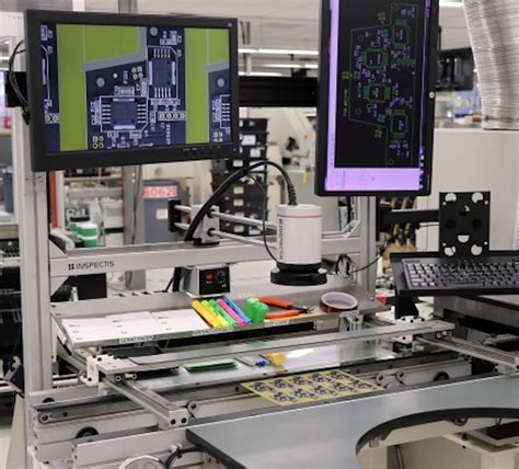
Automated Optical Inspection (AOI)
Automated Optical Inspection (AOI) is a more advanced form of visual inspection that uses cameras and image processing software to automatically detect defects. AOI systems can quickly scan the entire PCB and compare it to a reference image, flagging any deviations or anomalies.
AOI is particularly useful for detecting issues such as:
- Missing or misaligned components
- Solder defects (bridges, voids, insufficient solder)
- Incorrect component values or orientations
AOI systems can significantly speed up the inspection process and improve the accuracy and consistency of defect detection.
X-Ray Inspection
For PCBs with hidden or hard-to-see components, such as Ball Grid Arrays (BGAs) or flip chips, X-ray inspection may be necessary. X-ray systems use high-energy radiation to create images of the internal structure of the PCB, allowing operators to see through the board and inspect the solder joints and connections.
X-ray inspection is useful for detecting issues such as:
- Voids or cracks in BGA solder balls
- Misaligned or bridged connections under components
- Insufficient or excessive solder on hidden joints
X-ray inspection is a more specialized and expensive form of inspection but is essential for ensuring the quality of complex PCB assemblies.
In-Circuit Testing (ICT)
In-Circuit Testing (ICT) is a functional test that verifies the electrical connectivity and performance of the PCB. ICT systems use a bed-of-nails fixture to make contact with specific points on the PCB and test for shorts, opens, and other electrical faults.
ICT is useful for detecting issues such as:
- Short circuits or open connections
- Incorrect component values or tolerances
- Missing or incorrect components
ICT is a powerful tool for ensuring the electrical integrity of the PCB but requires specialized equipment and programming.

Common PCB Assembly Defects
During the final inspection, there are several common defects that operators should be on the lookout for. These include:
Solder Defects
Soldering is a critical step in PCB assembly, and defects in the solder joints can lead to reliability issues and failures. Common solder defects include:
- Bridges: When solder inadvertently connects two adjacent pads or traces.
- Voids: When there are gaps or holes in the solder joint, often due to insufficient solder or improper heating.
- Insufficient or excessive solder: When there is too little or too much solder on the joint, which can lead to weak connections or short circuits.
Solder defects can be detected through visual inspection, AOI, or X-ray inspection, depending on the location and severity of the defect.
Component Placement Defects
Incorrect component placement is another common issue in PCB assembly. This can include:
- Missing components: When a component is left off the board entirely.
- Misaligned components: When a component is not placed in the correct position or orientation.
- Incorrect component values: When the wrong value of component (e.g., resistor, capacitor) is used.
Component placement defects can be detected through visual inspection or AOI, and can often be corrected through rework or replacement.
Damaged Components or PCBs
During the assembly process, components or the PCB itself can become damaged due to handling, heat, or other factors. Common types of damage include:
- Bent or broken pins on through-hole components
- Cracked or chipped surface-mount components
- Delamination or warping of the PCB substrate
Damaged components or PCBs can be detected through visual inspection and may require rework or scrapping of the entire assembly.

Best Practices for PCB Inspection
To ensure a high-quality final product, there are several best practices that manufacturers should follow during the PCB inspection process:
Develop a Comprehensive Inspection Plan
Before beginning PCB assembly, manufacturers should develop a comprehensive inspection plan that outlines the types of inspections to be performed, the criteria for acceptance or rejection, and the documentation required. This plan should be based on the complexity of the PCB, the customer’s requirements, and any relevant industry standards.
Use a Combination of Inspection Methods
No single inspection method can catch all possible defects, so manufacturers should use a combination of visual inspection, AOI, X-ray, and ICT as appropriate. The specific methods used will depend on the complexity of the PCB and the types of components used.
Train and Certify Inspection Personnel
Inspection personnel should be properly trained and certified in the specific inspection methods and criteria used. This ensures that inspections are performed consistently and accurately, and that defects are properly identified and documented.
Document and Analyze Defects
When defects are identified during inspection, they should be properly documented and analyzed to determine the root cause. This can help identify process improvements that can prevent similar defects in the future.
Implement Statistical Process Control (SPC)
Statistical Process Control (SPC) is a method of monitoring and controlling the manufacturing process to ensure consistent quality. By tracking key metrics such as defect rates and yields, manufacturers can identify trends and make adjustments to the process as needed.

FAQ
What is the difference between AOI and visual inspection?
AOI (Automated Optical Inspection) uses cameras and image processing software to automatically detect defects, while visual inspection relies on a trained operator to visually examine the PCB. AOI is faster and more consistent than visual inspection but may not catch all types of defects.
How do manufacturers determine the acceptance criteria for PCB inspection?
The acceptance criteria for PCB inspection are typically based on industry standards, customer requirements, and the manufacturer’s own quality control policies. These criteria may include specifications for solder joint quality, component placement accuracy, and electrical performance.
Can all PCB defects be repaired?
Not all PCB defects can be repaired, depending on the type and severity of the defect. Some defects, such as solder bridges or component misalignments, can often be reworked. However, more severe defects such as damaged PCBs or incorrect component values may require scrapping the entire assembly.
How often should PCB inspection equipment be calibrated?
PCB inspection equipment, such as AOI machines and X-ray systems, should be regularly calibrated to ensure accurate and consistent results. The frequency of calibration will depend on the manufacturer’s recommendations and the usage of the equipment but is typically done at least annually.
What is the role of traceability in PCB inspection?
Traceability is the ability to track the history of a PCB assembly, including the materials used, the processes performed, and the inspection results. Traceability is important for identifying the root cause of defects, tracking the effectiveness of process improvements, and meeting regulatory requirements in some industries.
Conclusion
The final inspection of PCB assembly is a critical step in ensuring the quality and reliability of the final product. By using a combination of inspection methods, following best practices, and continuously improving the process, manufacturers can reduce defects, increase yields, and deliver high-quality PCBs to their customers.
| Inspection Method | Strengths | Weaknesses |
|---|---|---|
| Visual Inspection | Can catch obvious defects, low cost | Time-consuming, subject to human error |
| Automated Optical Inspection (AOI) | Fast, consistent, good for surface defects | Limited to visible defects, requires programming |
| X-Ray Inspection | Can detect hidden defects, e.g. in BGAs | Expensive, requires skilled operators |
| In-Circuit Testing (ICT) | Verifies electrical performance, can detect shorts/opens | Requires specialized fixtures, limited to accessible points |
Ultimately, the key to successful PCB inspection is a commitment to quality and continuous improvement. By staying up-to-date with the latest inspection technologies and best practices, manufacturers can deliver reliable, high-performance PCBs that meet the evolving needs of their customers.


Leave a Reply