Introduction to Via covering
Via covering is a crucial process in the manufacturing of printed circuit boards (PCBs) that involves filling or plugging the vias with a non-conductive material. Vias are small holes drilled through the layers of a PCB to create electrical connections between different layers. While vias are essential for the functionality of a PCB, they can also pose challenges during the manufacturing process and in the final application of the board.
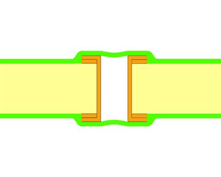
What are Vias?
Vias are tiny holes drilled through the layers of a PCB to create electrical connections between different layers. They allow signals and power to pass through the board, enabling the creation of complex circuits. There are several types of vias, including:
| Via Type | Description |
|---|---|
| Through Hole Via | Extends through all layers of the PCB |
| Blind Via | Connects an outer layer to an inner layer, but does not extend through the entire board |
| Buried Via | Connects inner layers without extending to the outer layers |
| Microvia | A small via with a diameter less than 150 microns |
Why is Via Covering Necessary?
Via covering is necessary for several reasons:
-
Preventing Solder Wicking: During the soldering process, molten solder can flow through the vias and create unwanted connections or short circuits. Via covering prevents this by sealing the vias before soldering.
-
Improving Signal Integrity: Uncovered vias can act as antennas, causing signal reflection and degrading signal integrity. By covering the vias, these issues can be mitigated.
-
Enhancing Mechanical Strength: Covered vias provide additional mechanical strength to the PCB, reducing the risk of damage during handling and in the final application.
-
Enabling Selective Plating: Via covering allows for selective plating of vias, which is useful for creating different types of vias (e.g., ground vias, power vias) on the same board.
Via Covering Methods
There are several methods for covering vias in PCBs, each with its own advantages and disadvantages. The choice of method depends on factors such as the size of the vias, the desired material properties, and the manufacturing capabilities.
Epoxy Filling
Epoxy filling involves dispensing a liquid epoxy resin into the vias and then curing it to create a solid plug. This method is suitable for large vias and provides good mechanical strength and thermal stability. However, epoxy filling can be time-consuming and may require additional processing steps.
Conductive Ink Filling
Conductive ink filling uses a conductive paste or ink to fill the vias. This method is suitable for creating conductive vias, such as those used for ground or power connections. The conductive ink is dispensed into the vias and then cured to create a solid, conductive plug. This method is faster than epoxy filling but may not provide the same level of mechanical strength.
Plugging with Preforms
Plugging with preforms involves inserting a solid, pre-shaped plug into the via. The preforms are typically made of a non-conductive material, such as silicone or plastic. This method is suitable for large vias and provides good mechanical strength and thermal stability. However, it can be more expensive than other methods and may require specialized equipment.
Tenting with Solder Mask
Tenting with solder mask involves applying a layer of solder mask over the vias to seal them. This method is suitable for small vias and is often used in conjunction with other covering methods. Tenting with solder mask is relatively simple and inexpensive but may not provide the same level of protection as other methods.

Via Covering Materials
The choice of via covering material depends on the specific requirements of the PCB and the manufacturing process. Some common materials used for via covering include:
Epoxy Resins
Epoxy resins are widely used for Via Filling due to their excellent mechanical strength, thermal stability, and adhesion properties. They are available in various formulations, including thermally conductive and electrically insulating variants. Epoxy resins can be cured using heat or ultraviolet (UV) light, depending on the specific formulation.
Conductive Inks and Pastes
Conductive inks and pastes are used for filling vias that require electrical conductivity, such as those used for ground or power connections. These materials typically consist of a conductive filler (e.g., silver, copper) dispersed in a polymer matrix. They can be cured using heat or UV light and provide good electrical conductivity and adhesion to the via walls.
Silicone and Plastic Preforms
Silicone and plastic preforms are solid, pre-shaped plugs used for plugging large vias. They provide good mechanical strength and thermal stability and are available in various shapes and sizes to accommodate different via dimensions. Preforms are typically inserted into the vias using specialized equipment and may require additional adhesive to ensure a secure fit.
Solder Mask
Solder mask is a polymer coating applied to the surface of a PCB to protect the copper traces and prevent solder bridging. It can also be used for tenting vias, providing a thin, insulating layer over the via openings. Solder mask is applied using screen printing or photoimaging techniques and can be cured using heat or UV light.

Via Covering Process
The via covering process typically involves the following steps:
-
Via Drilling: The vias are drilled through the layers of the PCB using a specialized drilling machine. The size and location of the vias are determined by the PCB design.
-
Cleaning: The drilled vias are cleaned to remove any debris or contaminants that may affect the covering process. This can be done using a variety of methods, such as plasma cleaning or chemical cleaning.
-
Filling or Plugging: The vias are filled or plugged with the chosen covering material using the appropriate method (e.g., epoxy filling, conductive ink filling, plugging with preforms).
-
Curing: The covering material is cured to create a solid, stable plug. The curing process depends on the specific material and may involve heat, UV light, or a combination of both.
-
Planarization: After curing, the surface of the PCB may be planarized to remove any excess covering material and ensure a smooth, level surface. This can be done using methods such as grinding or chemical mechanical polishing (CMP).
-
Inspection: The covered vias are inspected to ensure that they meet the required quality standards. This may involve visual inspection, electrical testing, or other methods.

Advantages of Via Covering
Via covering offers several advantages in the manufacturing and performance of PCBs:
-
Improved Reliability: By sealing the vias, via covering prevents solder wicking and other issues that can cause short circuits or other defects. This improves the overall reliability of the PCB.
-
Enhanced Signal Integrity: Covered vias reduce signal reflection and other issues that can degrade signal integrity, leading to better performance in high-frequency applications.
-
Increased Mechanical Strength: The covering material provides additional support and reinforcement to the vias, reducing the risk of damage during handling and in the final application.
-
Better Thermal Management: Some via covering materials, such as thermally conductive epoxies, can help dissipate heat from the PCB, improving thermal management and reducing the risk of overheating.
-
Enables Advanced PCB Designs: Via covering allows for the creation of more complex PCB designs with multiple layers and high-density interconnects. This is particularly important in applications such as 5G communication, where high-frequency signals and dense packaging are required.
Challenges and Considerations
While via covering offers many benefits, there are also some challenges and considerations to keep in mind:
-
Cost: Via covering can add to the overall cost of PCB manufacturing, particularly if specialized materials or equipment are required. The cost-benefit trade-off must be carefully considered for each application.
-
Manufacturing Complexity: Via covering adds additional steps to the PCB manufacturing process, which can increase complexity and lead time. This may require specialized equipment and expertise, which not all manufacturers may have.
-
Material Selection: The choice of via covering material must be carefully considered based on the specific requirements of the application, such as electrical properties, thermal stability, and mechanical strength. Improper material selection can lead to performance issues or reliability problems.
-
Process Control: The via covering process must be carefully controlled to ensure consistent quality and performance. This includes factors such as material dispense rate, curing temperature and time, and planarization parameters. Proper process control is essential for achieving reliable and repeatable results.
Future Trends in Via Covering
As PCB technology continues to advance, via covering is likely to play an increasingly important role in enabling new designs and applications. Some of the key trends and developments in via covering include:
-
Miniaturization: As PCBs become smaller and more densely packed, the size of vias is also decreasing. This requires new materials and methods for covering micro vias and other small features.
-
High-Frequency Applications: The demand for high-frequency PCBs is growing, driven by applications such as 5G communication, automotive radar, and high-speed data transfer. Via covering will be essential for maintaining signal integrity and reducing losses in these applications.
-
3D Packaging: 3D packaging technologies, such as package-on-package (PoP) and through-silicon via (TSV), are becoming increasingly popular for high-density applications. Via covering will play a critical role in enabling these technologies by providing reliable vertical interconnects between the different layers.
-
Sustainability: There is a growing focus on sustainability in PCB manufacturing, including the use of eco-friendly materials and processes. This may drive the development of new via covering materials that are more environmentally friendly and recyclable.
Conclusion
Via covering is a critical process in PCB manufacturing that involves filling or plugging the vias with a non-conductive material. It offers several benefits, including improved reliability, enhanced signal integrity, increased mechanical strength, and better thermal management. There are several methods and materials available for via covering, each with its own advantages and disadvantages.
As PCB technology continues to advance, via covering will play an increasingly important role in enabling new designs and applications. Miniaturization, high-frequency applications, 3D packaging, and sustainability are some of the key trends that will drive the development of new via covering solutions in the future.
By understanding the principles, methods, and materials involved in via covering, PCB designers and manufacturers can make informed decisions and optimize their processes for better performance, reliability, and cost-effectiveness.
Frequently Asked Questions (FAQ)
-
What is the purpose of via covering in PCBs?
Via covering serves several purposes, including preventing solder wicking, improving signal integrity, enhancing mechanical strength, and enabling selective plating. -
What are the most common methods for via covering?
The most common methods for via covering are epoxy filling, conductive ink filling, plugging with preforms, and tenting with solder mask. The choice of method depends on factors such as via size, desired material properties, and manufacturing capabilities. -
What materials are used for via covering?
Common materials used for via covering include epoxy resins, conductive inks and pastes, silicone and plastic preforms, and solder mask. The choice of material depends on the specific requirements of the PCB and the manufacturing process. -
How does via covering improve signal integrity in high-frequency applications?
Uncovered vias can act as antennas, causing signal reflection and degrading signal integrity. By covering the vias, these issues can be mitigated, leading to better performance in high-frequency applications. -
What are some of the challenges and considerations in via covering?
Some of the challenges and considerations in via covering include cost, manufacturing complexity, material selection, and process control. Proper planning and optimization are necessary to achieve reliable and cost-effective via covering solutions.


Leave a Reply