Why is Via Filling Important?
Via filling plays a crucial role in the production of modern PCBs for several reasons:
-
Electrical Connectivity: By filling the vias with conductive material, electrical signals and power can be transmitted between the different layers of the PCB, enabling the creation of complex, high-density designs.
-
Mechanical Strength: Filled vias provide additional mechanical support to the PCB, reducing the risk of damage during handling and assembly, and improving the overall durability of the board.
-
Thermal Management: Filled vias can help dissipate heat generated by components on the PCB, preventing overheating and ensuring optimal performance.
-
Signal Integrity: Properly filled vias minimize signal distortion and reflections, maintaining signal integrity in high-speed and high-frequency applications.
-
Manufacturing Efficiency: Via filling allows for the creation of smaller, more compact PCB designs, reducing material costs and improving manufacturing efficiency.
Via Filling Methods
There are several methods used for via filling, each with its own advantages and disadvantages. The choice of method depends on factors such as the PCB design, the required performance characteristics, and the manufacturing capabilities of the PCB fabricator.
Electroplating
Electroplating is one of the most common methods for via filling. In this process, the PCB is immersed in an electrolytic solution containing the desired conductive material, typically copper. An electric current is applied, causing the copper ions to migrate and deposit onto the walls of the vias, gradually filling them.
Advantages of electroplating include:
– High conductivity of the filled vias
– Uniform filling of vias across the board
– Compatibility with a wide range of PCB designs and materials
Disadvantages of electroplating include:
– Relatively slow process compared to other methods
– Requires specialized equipment and expertise
– May not be suitable for very small or high aspect ratio vias
Screen Printing
Screen printing involves using a stencil or screen to apply a conductive paste, such as silver or copper-filled epoxy, onto the surface of the PCB and into the vias. The paste is then cured using heat, creating a solid, conductive filling.
Advantages of screen printing include:
– Fast and cost-effective process
– Suitable for large-scale production
– Can fill vias of various sizes and shapes
Disadvantages of screen printing include:
– Lower conductivity compared to electroplating
– May require multiple passes to achieve complete filling
– Possible voiding or air pockets in the filled vias
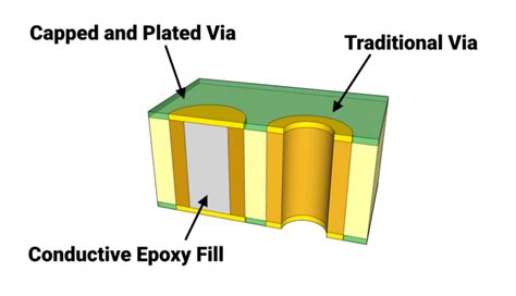
Conductive Ink Filling
Conductive ink filling is a newer method that uses specialized inks containing conductive particles, such as silver or copper, to fill the vias. The ink is dispensed into the vias using a needle or nozzle, and then cured using heat or UV light.
Advantages of conductive ink filling include:
– Fast and efficient process
– Suitable for small and high aspect ratio vias
– Minimal waste and cleaning required
Disadvantages of conductive ink filling include:
– Higher material costs compared to other methods
– Limited compatibility with certain PCB materials and finishes
– Possible variations in conductivity and filling quality

Via Filling Process
The via filling process typically involves several steps, regardless of the specific method used. These steps ensure that the vias are properly prepared, filled, and finished to achieve the desired performance characteristics.
-
Drilling: Vias are drilled through the PCB using specialized equipment, creating the holes that will be filled with conductive material.
-
Cleaning: The drilled vias are cleaned to remove any debris or contaminants that could affect the filling process or the final performance of the filled vias.
-
Pre-treatment: Depending on the filling method and the PCB material, the vias may require pre-treatment, such as desmearing or activation, to improve adhesion and ensure complete filling.
-
Filling: The vias are filled with conductive material using one of the methods described above (electroplating, screen printing, or conductive ink filling).
-
Curing: The filled vias are cured using heat or UV light to solidify the conductive material and create a permanent, stable connection.
-
Planarization: In some cases, the filled vias may require planarization, or leveling, to ensure a smooth and even surface for subsequent manufacturing steps, such as applying solder mask or surface finishes.
-
Inspection: The filled vias are inspected to verify that they meet the required quality standards, such as complete filling, adequate conductivity, and absence of defects.

Factors Affecting Via Filling Quality
Several factors can influence the quality and performance of filled vias, and it is essential to consider these factors when designing and manufacturing PCBs.
Via Size and Aspect Ratio
The size and aspect ratio of the vias can significantly impact the filling process and the final quality of the filled vias. Aspect ratio refers to the ratio of the via’s depth to its diameter. Higher aspect ratios (deeper and narrower vias) are more challenging to fill completely and uniformly.
| Via Diameter (mm) | Via Depth (mm) | Aspect Ratio |
|---|---|---|
| 0.2 | 0.6 | 3:1 |
| 0.1 | 0.6 | 6:1 |
| 0.05 | 0.6 | 12:1 |
As the table above illustrates, smaller via diameters result in higher aspect ratios, making the filling process more difficult. PCB designers must consider the capabilities of the manufacturing process and choose via sizes and aspect ratios that can be reliably filled.
PCB Material and Surface Finish
The PCB material and surface finish can also affect the via filling process and the adhesion of the conductive material to the via walls. Some materials, such as high-frequency laminates or flexible substrates, may require special considerations or pre-treatment to ensure proper filling.
Common PCB surface finishes, such as ENIG (Electroless Nickel Immersion Gold) or OSP (Organic Solderability Preservative), can also impact the filling process. For example, ENIG may require additional cleaning or activation steps to ensure good adhesion of the conductive material.
Filling Material Properties
The properties of the filling material, such as viscosity, particle size, and conductivity, can influence the filling process and the final performance of the filled vias.
| Filling Material | Viscosity (cP) | Particle Size (µm) | Conductivity (% IACS) |
|---|---|---|---|
| Copper Paste | 50,000-200,000 | 5-20 | 40-60 |
| Silver Epoxy | 10,000-50,000 | 1-10 | 60-80 |
| Conductive Ink | 1,000-10,000 | 0.1-5 | 20-40 |
Lower viscosity materials may be easier to dispense and fill the vias, but they may also be more prone to voiding or leakage. Smaller particle sizes can improve the filling of narrow vias but may also increase the cost of the material. Higher conductivity materials, such as silver epoxy, can provide better electrical performance but may also be more expensive.

Testing and Inspection of Filled Vias
To ensure the quality and reliability of filled vias, several testing and inspection methods are used during the PCB manufacturing process.
Cross-Sectioning
Cross-sectioning involves cutting the PCB along the filled vias and examining the cross-section under a microscope. This destructive test allows for the visual inspection of the filling quality, including the presence of voids, cracks, or incomplete filling.
Resistance Testing
Resistance testing measures the electrical resistance of the filled vias using a multimeter or a dedicated resistance tester. This non-destructive test verifies that the filled vias have adequate conductivity and can carry the required current.
Thermal Cycling
Thermal cycling exposes the PCB to repeated cycles of high and low temperatures to simulate the stresses encountered during operation. This test helps evaluate the mechanical integrity and reliability of the filled vias under varying thermal conditions.
Microsectioning
Microsectioning is another destructive test that involves cutting the PCB into small sections and examining the filled vias under high magnification. This method provides detailed information about the filling quality, adhesion, and any defects present in the filled vias.
Frequently Asked Questions (FAQ)
- What is the difference between through-hole vias and blind/buried vias?
-
Through-hole vias extend through the entire thickness of the PCB, connecting all layers. Blind vias connect an outer layer to an inner layer, while buried vias connect inner layers without extending to the outer layers.
-
Can all PCB designs benefit from via filling?
-
Via filling is most beneficial for high-density, multi-layer PCBs used in demanding applications, such as aerospace, defense, and high-speed digital devices. Simple, low-layer count designs may not require via filling.
-
How does via filling affect the cost and lead time of PCB manufacturing?
-
Via filling can increase the cost and lead time of PCB manufacturing due to the additional processing steps and materials required. However, the benefits of via filling, such as improved reliability and performance, often outweigh the increased costs for critical applications.
-
What are the most common defects encountered in via filling, and how can they be prevented?
-
Common defects include voids, incomplete filling, and poor adhesion. These defects can be prevented by selecting the appropriate filling method, ensuring proper via preparation and cleaning, and optimizing the filling process parameters.
-
Can filled vias be reworked or repaired if defects are discovered after manufacturing?
- Reworking or repairing filled vias can be challenging and may not always be possible, depending on the extent and location of the defects. In some cases, the defective vias may need to be drilled out and refilled, or the entire PCB may need to be scrapped and remade.
Conclusion
Via filling is a critical process in the manufacturing of high-density, multi-layer PCBs, ensuring reliable electrical connections, mechanical strength, and optimal performance. The choice of via filling method, such as electroplating, screen printing, or conductive ink filling, depends on various factors, including the PCB design, required performance characteristics, and manufacturing capabilities.
To achieve the best results, PCB designers and manufacturers must consider factors such as via size and aspect ratio, PCB material and surface finish, and filling material properties. Thorough testing and inspection, using methods like cross-sectioning, resistance testing, thermal cycling, and microsectioning, are essential for verifying the quality and reliability of filled vias.
As electronic devices continue to advance in complexity and performance, via filling will remain a vital aspect of PCB manufacturing, enabling the creation of compact, high-density, and reliable electronic systems across a wide range of industries and applications.


Leave a Reply