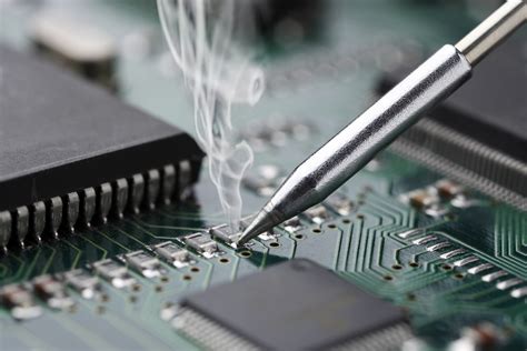
What is PCB Assembly?
PCB assembly is the process of soldering or mounting electronic components onto a printed circuit board (PCB). The main steps in PCB assembly include:
- Solder Paste Application
- Pick and Place
- Reflow Soldering
- Inspection and Quality Control
PCB assembly can be done manually for simple boards and low volumes, or automated using pick-and-place machines and reflow ovens for complex designs and high volumes. Proper PCB assembly ensures good electrical connections, component alignment, and reliability of the final product.
PCB Assembly Methods
There are two main PCB assembly methods:
| Method | Description |
|---|---|
| Through-Hole Technology (THT) | Components have long leads that are inserted into holes drilled in the PCB and soldered to pads on the opposite side |
| Surface-Mount Technology (SMT) | Components are placed and soldered directly onto pads on the surface of the PCB |
SMT is more common for modern PCB designs as it enables smaller components and higher density compared to through-hole. However, some through-hole components are still used when needed.
PCB Assembly Services
Many companies offer PCB assembly services, ranging from simple prototype assembly to full turnkey production. When choosing a PCB assembly partner, consider factors such as:
- Technical capabilities (component sizes, board complexity, etc.)
- Quality certifications (ISO 9001, IPC class 2/3, etc.)
- Lead times and flexibility
- Pricing and minimum order quantities
- Location and supply chain
Look for an experienced assembly partner that can handle your technical requirements and business needs. Clear communication and attention to detail are key to a successful assembly project.
STANDARD pool PCB Assembly
STANDARD pool PCB assembly is a cost-effective option for small to medium volumes. In this service model, multiple customers’ PCB designs are “pooled” together to fill up standard panel sizes. This allows PCB manufacturers to produce boards more efficiently and pass the savings to customers.
Key features of STANDARD pool PCB assembly:
- Low to medium volumes (typically 50-5000 pieces)
- Cost savings from 30-50% compared to on-demand
- Standard specs and stackups
- Longer lead times (2-4 weeks)
- Limited customization and engineering support
STANDARD pool works well for simpler 2-4 layer designs within standard specifications. For complex, high-density, or highly customized designs, on-demand assembly is recommended for greater flexibility and support.

Preparing Your Design for Assembly
To ensure a smooth assembly process, properly prepare your design package with all the necessary files and information, such as:
- Bill of Materials (BOM): List of components
- Gerber files: PCB fabrication data
- Centroid or pick-and-place (PnP) file: Component placement data
- Assembly drawings: Visual aids and instructions
- Special requirements: Packaging, testing, etc.
Make sure the BOM matches your schematic and layout. Include manufacturer part numbers (MPNs), quantities, and reference designators for each component. Ensure the Gerber and centroid files are up to date with the correct board revision.
Design for Assembly (DFA)
Following good DFA principles will help avoid assembly issues and improve yield:
- Use standard component sizes and pitches when possible
- Provide adequate spacing between components for pick-and-place
- Minimize use of through-hole or odd-form components
- Specify a solder mask to prevent bridging
- Add fiducials to aid machine vision alignment
- Choose packaging to protect components and aid assembly (reels, trays, etc.)
Work with your assembly partner early in the design process to identify any DFA optimizations. Simple adjustments can often greatly improve manufacturability and reduce cost.

PCB Assembly Process Flow
A typical PCB assembly process flow consists of the following steps:
-
Incoming Inspection: PCBs, components, and materials are received and checked for quality and accuracy.
-
Solder Paste Printing: Solder paste is applied to the PCB pads through a stencil using a precise printer.
-
Pick and Place: A pick-and-place machine automatically picks up components from reels or trays and places them onto their corresponding locations on the PCB.
-
Reflow Soldering: The PCB goes through a reflow oven which melts the solder paste, forming permanent solder joints between the components and PCB pads.
-
Inspection: Automated optical inspection (AOI) checks for missing components, alignment, and solder defects. X-ray inspection may be used for hidden joints like BGAs.
-
Through-hole Assembly: Any through-hole components are manually inserted and wave soldered, or selectively soldered using mini-waves or fountains.
-
Cleaning: Flux residues are cleaned off the PCB if necessary using various cleaning agents.
-
Test and Inspection: Functional circuit testing, boundary scan, and visual inspection are performed to verify the assembled PCB is complete and working properly.
-
Conformal Coating: A protective coating may be applied to shield the PCB from moisture and contaminants.
-
Final Inspection and Packaging: The PCBs undergo a final visual inspection and are packaged according to customer requirements (ESD bags, trays, boxes, etc.)
Throughout the process, various quality control measures are taken to inspect, test, and ensure the PCBs are built to spec.

Conclusion
In summary, PCB assembly is a crucial step that brings a circuit design to life as a functional product. Choosing the right assembly partner and service level depends on your technical needs, volume, and budget.
STANDARD pool assembly provides cost savings for simpler designs in low to medium volumes. Proper design preparation and communication with your assembler are essential for success.
As PCB designs continue to push the limits of density and complexity, strategic assembly partnerships will play an increasingly important role in bringing innovative electronics to market.
Frequently Asked Questions
What is the typical turnaround time for PCB assembly?
Turnaround times vary depending on the service level, complexity, and order size. STANDARD pool assembly usually takes 2-4 weeks, while on-demand assembly can range from a few days to a few weeks.
What are the common PCB Surface Finishes and their trade-offs?
Common surface finishes include HASL (Hot Air Solder Leveling), lead-free HASL, ENIG (Electroless Nickel Immersion Gold), and OSP (Organic Solderability Preservative). HASL is economical but not as flat. ENIG has excellent flatness and shelf life but is more expensive. OSP is a good middle ground for many applications.
How much does PCB Assembly Cost?
PCB Assembly Costs depend on the number of components, component types, placement volume, testing requirements, and setup fees. Simpler assemblies can start at a few dollars per board for medium volumes. Always get a quote for your specific design and quantity.
What are some common PCB assembly defects?
Common assembly defects include tombstoning (one end of a component lifts up), bridging (solder shorts between pins), insufficient solder, skewed or missing components, and damaged components. Following good DFA practices and having solid process controls minimize the risk of defects.
Do I need to include all parts for PCB assembly?
Yes, generally you need to provide all the components for assembly, either by shipping them to the assembler or having them procured on your behalf. Some assembly shops offer kitting services to source and manage components for you. Communicate clearly what parts you are providing versus what you need them to procure.


Leave a Reply