Introduction to Surface Mount Devices
Surface Mount Devices, commonly known as SMDs, are electronic components that are designed to be mounted directly onto the surface of a printed circuit board (PCB). Unlike through-hole components, which require leads to be inserted into holes drilled in the PCB, SMDs are soldered directly onto the board’s surface. This technology has revolutionized the electronics industry by enabling the production of smaller, lighter, and more efficient electronic devices.
Advantages of Surface Mount Devices
- Miniaturization: SMDs allow for the creation of smaller electronic devices due to their compact size and the elimination of through-hole leads.
- Increased Functionality: With SMDs, more components can be placed on a single PCB, enabling the development of complex circuits with enhanced functionality.
- Improved Reliability: SMDs have shorter leads and are directly soldered to the PCB, reducing the risk of mechanical and electrical issues caused by lead damage or poor connections.
- Cost-Effective: The automated assembly process for SMDs is faster and more efficient than through-hole component assembly, reducing manufacturing costs.
Types of Surface Mount Devices
There are several types of SMDs, each with its own unique characteristics and applications. Some of the most common types include:
1. Resistors
Surface mount resistors are passive components that provide electrical resistance in a circuit. They are available in various sizes, power ratings, and resistance values. The most common package sizes for SMD resistors are:
| Package Size | Dimensions (mm) | Power Rating (W) |
|---|---|---|
| 0201 | 0.6 x 0.3 | 0.05 |
| 0402 | 1.0 x 0.5 | 0.063 |
| 0603 | 1.6 x 0.8 | 0.1 |
| 0805 | 2.0 x 1.25 | 0.125 |
| 1206 | 3.2 x 1.6 | 0.25 |
2. Capacitors
SMD capacitors are passive components that store electrical energy in an electric field. They are used for various purposes, such as filtering, coupling, and decoupling. SMD capacitors come in different types, including ceramic, tantalum, and aluminum electrolytic capacitors.
3. Inductors
Surface mount inductors are passive components that store energy in a magnetic field when an electric current flows through them. They are used for filtering, power supply regulation, and impedance matching. SMD inductors are available in various sizes and inductance values.
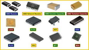
4. Integrated Circuits (ICs)
SMD integrated circuits are complex electronic components that contain multiple transistors, resistors, capacitors, and other elements on a single chip. They perform specific functions, such as amplification, signal processing, and memory storage. SMD ICs come in a wide range of package types, such as:
- Small Outline Integrated Circuit (SOIC)
- Quad Flat Package (QFP)
- Ball Grid Array (BGA)
- Land Grid Array (LGA)
5. Diodes
Surface mount diodes are semiconductor devices that allow current to flow in only one direction. They are used for rectification, voltage regulation, and Circuit Protection. SMD diodes are available in various types, such as signal diodes, Zener Diodes, and Schottky diodes.

SMD Packaging and Labeling
SMDs are packaged in various ways to protect the components and facilitate automated assembly. Some common SMD packaging types include:
- Tape and Reel: Components are placed in pockets on a continuous tape, which is wound onto a reel. This packaging method is suitable for high-volume, automated assembly processes.
- Cut Tape: Similar to tape and reel packaging, but the tape is cut into shorter lengths for smaller production runs or manual assembly.
- Bulk: Components are loosely packed in a container, such as a bag or a box. This packaging method is suitable for low-volume production or prototyping.
SMDs are often labeled with a code that indicates their value, tolerance, and other characteristics. These codes can vary depending on the manufacturer and the type of component. For example, SMD resistors use a three- or four-digit code that represents their resistance value, while capacitors use a three-digit code that represents their capacitance value in picofarads.

PCB Design Considerations for SMDs
When designing a PCB for SMDs, several factors must be taken into account to ensure proper component placement, soldering, and overall circuit performance.
1. Footprint and Land Pattern
Each SMD has a specific footprint, which is the pattern of pads on the PCB that matches the component’s leads or terminals. The land pattern is the copper area surrounding the pads, which provides a surface for soldering and heat dissipation. It is essential to use the correct footprint and land pattern for each component to ensure proper fit and reliable connections.
2. Solder Mask and Paste
A solder mask is a protective layer applied to the PCB that prevents solder from bridging between adjacent pads or traces. Solder paste is a mixture of tiny solder particles and flux that is applied to the pads before component placement. The amount of solder paste used must be carefully controlled to avoid insufficient or excessive solder joints.
3. Component Placement and Orientation
SMDs must be placed on the PCB with the correct orientation and alignment to ensure proper functionality and avoid short circuits. Automated pick-and-place machines are often used for high-volume production, while manual placement may be used for low-volume or prototype builds. It is essential to follow the component manufacturer’s recommendations for placement and orientation.
4. Thermal Considerations
SMDs generate heat during operation, which must be dissipated to prevent component damage and ensure reliable performance. PCB designers must consider factors such as copper pour, thermal vias, and heat sinks to manage heat dissipation effectively. Proper layout and component spacing can also help minimize thermal issues.

Assembly and Soldering Techniques for SMDs
The assembly and soldering of SMDs require specialized techniques and equipment to ensure reliable connections and prevent component damage.
1. Solder Paste Application
Solder paste is typically applied to the PCB using a stencil, which is a thin metal sheet with openings that match the component pads. The stencil is placed over the PCB, and solder paste is spread across the surface, filling the openings. Alternatively, solder paste can be applied using a dispenser or syringe for small-scale or prototype assembly.
2. Pick-and-Place Machine
For high-volume production, an automated pick-and-place machine is used to place SMDs onto the PCB. The machine uses a vacuum nozzle to pick up components from feeders or trays and place them on the solder paste-coated pads with high precision and speed.
3. Reflow Soldering
After component placement, the PCB undergoes reflow soldering, which involves heating the board in a controlled manner to melt the solder paste and form permanent connections between the components and the pads. Reflow soldering is typically performed using a convection oven or an infrared heating system, following a specific temperature profile to ensure proper solder joint formation.
4. Inspection and Rework
After soldering, the PCB is inspected for defects such as bridging, insufficient solder, or misaligned components. Automated optical inspection (AOI) systems are often used for high-volume production, while manual inspection may be used for small-scale or prototype assembly. If defects are found, rework may be necessary, which involves removing and replacing the affected components using specialized tools and techniques.
Advantages of SMDs in Modern Electronics
The widespread adoption of SMDs in modern electronics has brought about numerous benefits, including:
- Miniaturization: SMDs have enabled the development of smaller, more compact electronic devices, such as smartphones, wearables, and IoT sensors.
- Increased Functionality: With more components fitting on a single PCB, SMDs have allowed for the creation of more complex and feature-rich electronic devices.
- Improved Reliability: The direct soldering of SMDs to the PCB reduces the risk of mechanical and electrical issues, resulting in more reliable electronic products.
- Cost Reduction: The automated assembly process for SMDs is faster and more efficient than through-hole component assembly, reducing manufacturing costs and enabling mass production of affordable electronic devices.
- Enhanced Performance: SMDs have shorter leads and are mounted closer to the PCB, reducing parasitic inductance and capacitance, which can improve signal integrity and high-frequency performance.
Future Trends in SMD Technology
As electronic devices continue to evolve and become more advanced, SMD technology is expected to keep pace with new developments and innovations.
1. Miniaturization
The trend towards smaller and more compact electronic devices is likely to drive the development of even smaller SMDs. Advances in packaging technologies, such as chip-scale packaging (CSP) and wafer-level packaging (WLP), may enable the creation of ultra-miniature components.
2. High-Density Interconnect (HDI)
HDI PCBs, which feature finer traces, smaller vias, and higher component density, are becoming increasingly popular in advanced electronic applications. SMDs play a crucial role in enabling HDI designs by providing compact, high-performance components that can be closely spaced on the PCB.
3. Advanced Materials
New materials, such as high-temperature ceramics and low-loss dielectrics, may be incorporated into SMDs to improve their performance and reliability in demanding applications, such as automotive electronics and aerospace systems.
4. Embedded Components
The integration of SMDs directly into the PCB substrate, known as embedded component technology, is an emerging trend that can further reduce the size and improve the performance of electronic devices. By embedding components within the PCB Layers, designers can achieve higher component density and shorter signal paths.
5. Additive Manufacturing
Additive manufacturing techniques, such as 3D printing, may be used to fabricate SMDs and PCBs in the future. This technology could enable the rapid prototyping and customization of electronic components and assemblies, as well as the creation of complex geometries and multi-functional structures.
Frequently Asked Questions (FAQ)
-
What is the difference between SMDs and through-hole components?
SMDs are mounted directly onto the surface of a PCB, while through-hole components have leads that are inserted into holes drilled in the PCB and soldered on the opposite side. -
Can SMDs be soldered by hand?
Yes, SMDs can be soldered by hand using a fine-tipped soldering iron and tweezers. However, hand soldering can be challenging due to the small size of the components and the need for precise control. It is more common for SMDs to be soldered using automated reflow soldering processes. -
Are SMDs more expensive than through-hole components?
In general, SMDs are less expensive than their through-hole counterparts due to the automated assembly process and the reduced material cost. However, the cost of an individual SMD may be higher than a through-hole component with the same functionality. -
Can SMDs be replaced if they fail?
Yes, SMDs can be replaced using specialized rework tools and techniques. The process involves removing the defective component, cleaning the pads, and soldering a new component in its place. However, rework can be challenging and time-consuming, especially for fine-pitch components. -
Are there any disadvantages to using SMDs?
While SMDs offer many benefits, there are some potential disadvantages to consider. These include the need for specialized assembly equipment, the difficulty of manual soldering and rework, and the potential for thermal stress and mechanical damage due to the small size and close spacing of the components.
Conclusion
Surface Mount Devices have revolutionized the electronics industry by enabling the production of smaller, lighter, and more efficient electronic devices. SMDs come in various types, packages, and sizes, each with its own unique characteristics and applications. When designing PCBs for SMDs, careful consideration must be given to factors such as footprint, land pattern, solder mask, and thermal management. The assembly and soldering of SMDs require specialized techniques and equipment, such as solder paste application, pick-and-place machines, and reflow soldering. As electronic devices continue to advance, SMD technology is expected to evolve, with trends towards further miniaturization, high-density interconnect, advanced materials, embedded components, and additive manufacturing. By understanding the fundamentals of SMDs and their role in modern electronics, engineers and technicians can design, manufacture, and troubleshoot electronic devices with greater efficiency and reliability.


Leave a Reply