Introduction to Zener Diodes and the 1N4732A
A Zener diode is a special type of diode that allows current to flow in the forward direction like a normal diode, but also in the reverse direction if the voltage is larger than the breakdown voltage known as “Zener knee voltage” or “Zener voltage”. A Zener diode is therefore ideal for applications requiring a precise reference voltage or for protection from overvoltage.
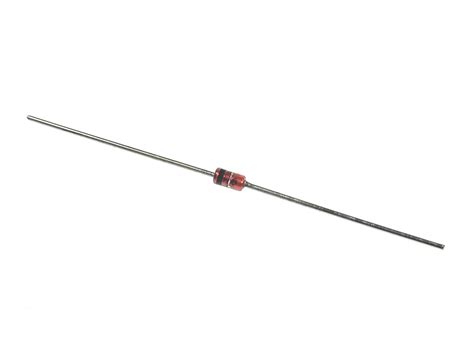
The 1N4732A is a popular 4.7V Zener diode in a DO-41 glass package. It is designed for voltage regulation, voltage reference, and surge protection applications in consumer, industrial and automotive electronics.
Key Specifications of the 1N4732A Zener Diode
| Parameter | Value |
|---|---|
| Zener Voltage (Vz) @ Izt | 4.7V |
| Zener Impedance (Zzt) @ Izt | 10 Ohms |
| Zener Current (Izt) | 49 mA |
| Maximum Power Dissipation (Pd) | 1W |
| Reverse Current (Ir) @ Vr = 4V | 5 uA |
| Operating Temperature Range | -65 to 200 °C |
The 1N4732A has a nominal Zener voltage of 4.7V at a test current of 49mA. The maximum Zener impedance at this current is 10 Ohms. The diode can handle up to 1W of power dissipation and has a low 5 uA reverse leakage current at 4V. It can operate over a wide -65 to 200°C temperature range.
How a Zener Diode Works
A Zener diode is like a normal PN junction diode but is designed and manufactured to optimize the Zener breakdown effect. In forward bias mode, it conducts current like a regular diode once the forward voltage exceeds about 0.7V. However, in reverse bias, a small leakage current flows until the reverse voltage reaches the Zener breakdown voltage point (Vz). At this point, the diode allows a large current to flow while maintaining an almost constant voltage drop.
The Zener breakdown occurs due to quantum tunneling of electrons from the valence band to the conduction band in the heavily doped PN junction under high reverse electric fields. This allows the Zener diode to act as a voltage reference or regulator.
Zener Diode I-V Characteristics
The current-voltage (I-V) characteristics of a Zener diode show its unique behavior:
        Forward  |   Reverse
           ->|   |<-
              Vz
               |
               |
             __|__
            /  |  \
           /   |   \
          /    |    \
In the forward direction, it acts like a normal diode, conducting once the voltage exceeds the diode’s forward voltage drop (about 0.7V). In reverse, only a small leakage current flows until the Zener voltage Vz is reached, at which point the current increases dramatically while the voltage stays nearly constant at Vz.

Applications of the 1N4732A Zener Diode
The key properties of the 1N4732A – its well-defined 4.7V reverse breakdown voltage, low Zener impedance, ability to handle high power, and wide operating temperature range – make it suitable for several important applications:
Voltage Regulation
One of the most common uses of the 1N4732A is as a simple voltage regulator to provide a stable 4.7V reference voltage from a higher, fluctuating input voltage.
A basic 4.7V regulator using the 1N4732A looks like:
                  1N4732A
   Unregulated    +-|>|-+
   DC Input       |     |
  (5-20V) ----R1--+     +---- Regulated 4.7V Output
                        |
                       === C1
                        |
                       GND
R1 is chosen to set the Zener current at 5-10 mA, within the diode’s optimum operating range but well below its 49 mA test current limit. Capacitor C1 filters any noise on the output.
For example, with a 12V input, setting the Zener current to 5 mA requires:
R1 = (Vin – Vz) / Iz
= (12V – 4.7V) / 5mA
= 1.46 kOhm
So a standard 1.5 kOhm resistor would be suitable for R1.
Voltage Reference
The stable 4.7V from the 1N4732A also makes a good voltage reference for analog-to-digital converters, comparators, and other precision circuits needing an accurate voltage reference point.
The 1N4732A provides a lower-cost, lower-precision alternative to dedicated voltage reference ICs in applications that can tolerate its ±5% tolerance on Vz. Multiple 1N4732As can be stacked in series for higher reference voltages in multiples of 4.7V.
Overvoltage Protection
The 1N4732A’s Zener breakdown characteristic allows it to act as a surge suppressor to protect sensitive electronics from voltage spikes. When connected in parallel with the circuit to be protected, it acts as a shunt, conducting excess current to ground when the voltage exceeds Vz.
A simple overvoltage protection circuit using the 1N4732A looks like:
                 1N4732A  Protected
   Input       +-|>|-+    Circuit
  -----R1------+     +------
                           |
                          GND
R1 limits the current through the diode during a surge. For example, to protect a 5V circuit from spikes up to 100V with a maximum current of 1A, R1 should be:
R1 = (Vmax – Vz) / Imax
= (100V – 4.7V) / 1A
= 95.3 Ohms
A standard 100 Ohm, >1W resistor would be suitable.

Handling and Using the 1N4732A
Mounting and Thermal Considerations
With its glass DO-41 package, the 1N4732A looks like a typical small signal diode but can dissipate up to 1W. This high power capability for its size means careful circuit board layout is needed to prevent overheating.
The diode’s leads provide a thermal path to dissipate heat, so avoid trimming them shorter than necessary. For power dissipation over 0.5W or operation at high ambient temperatures, use a heat sink. A large copper PCB pad or plane connected to the cathode lead also helps conduct heat away.
Soldering Guidelines
The 1N4732A’s glass package is more sensitive to thermal shock than plastic-packaged diodes. Follow these guidelines when soldering:
- Use a temperature controlled soldering iron set no higher than 260°C.
- Contact the lead to be soldered with the iron before applying solder.
- Limit soldering time to 3 seconds per lead.
- Allow the device to cool down before soldering the second lead.
- Avoid putting mechanical stress on the leads.
Protection Recommendations
The 1N4732A doesn’t have built-in protection against repetitive surge currents or electrostatic discharge (ESD). For applications with these hazards, add external protection or choose a more robust Zener diode.
A series resistor can limit current during repeated surges. Transient voltage suppression (TVS) diodes in parallel with the 1N4732A clamp short overvoltage spikes. Do not exceed the diode’s 1W power dissipation rating for longer than a few milliseconds.

FAQ
What happens if I operate a 1N4732A above its power dissipation rating?
Exceeding the maximum power dissipation of 1W will cause the diode to overheat. Initially, its Zener voltage will drift outside the datasheet specifications. If the overload is sustained or severe enough, the device will be permanently damaged, leading to a short or open circuit. Always limit current to a safe level.
Can I get a tighter tolerance on the Zener voltage than ±5%?
The 1N4732A is not available with a tighter tolerance. For more precise voltage references, use a dedicated voltage reference IC or select a Zener diode with a lower tolerance like the 1N4370A (4.7V ±2%). Generally, tighter tolerance diodes cost more.
Is the 1N4732A suitable for temperature sensing?
No. While its Zener voltage does vary slightly with temperature, the 1N4732A is not intended or characterized for use as a temperature sensor. Its temperature coefficient is not specified or guaranteed. For temperature sensing, use a dedicated silicon, thermistor, RTD, or Thermocouple Sensor.
Can I use a 1N4732A in a voltage regulator with more than 1W output?
The 1N4732A is limited to 1W power dissipation so it is not suitable as a regulator pass device for more than about 200 mA output current. For higher power, use a Zener diode with a higher power rating like the 1N4739A (4.7V, 5W), or add a pass transistor and heatsink to the regulator circuit.
What is the shelf life of the 1N4732A? Will its performance degrade over time?
The 1N4732A has an indefinite shelf life under proper storage conditions. Its glass-passivated junction is stable and its electrical characteristics do not degrade significantly over time. Proper storage means keeping the devices in a cool, dry environment away from direct sunlight, preferably in their original sealed packaging. Moisture, corrosive atmospheres, and extreme temperatures can degrade the leads or package and affect solderability over extended periods.


Leave a Reply