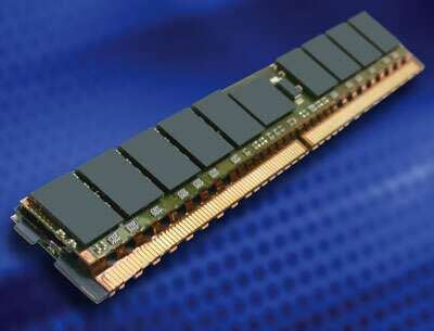
Introduction to DDR2 and PCB Design
DDR2 (Double Data Rate 2) is a type of synchronous dynamic random-access memory (SDRAM) that has been widely used in computer systems since its introduction in 2003. DDR2 operates at higher clock speeds and provides faster data transfer rates compared to its predecessor, DDR. When designing PCBs for DDR2 memory, signal integrity is a critical factor to ensure reliable performance and minimize potential issues such as signal reflections, crosstalk, and noise.
In this article, we will explore the key considerations for PCB signal integrity design when working with DDR2 800, a specific variant of DDR2 memory that operates at a clock frequency of 400 MHz (effective 800 MT/s). We will discuss the importance of proper PCB layout, signal routing, termination strategies, and other techniques to optimize signal quality and ensure robust DDR2 memory interfaces.
Understanding DDR2 800 Specifications
DDR2 800 is a high-speed memory interface that offers a data transfer rate of 6400 MB/s (mega bytes per second). It achieves this by operating at a clock frequency of 400 MHz and utilizing both the rising and falling edges of the clock signal to transfer data. The key specifications of DDR2 800 are summarized in the table below:
| Parameter | Value |
|---|---|
| Clock Frequency | 400 MHz |
| Data Rate | 800 MT/s |
| Prefetch | 4 bits |
| Voltage | 1.8V |
| DRAM Core Voltage | 1.8V |
| I/O Voltage | 1.8V |
| On-Die Termination (ODT) | 150 ohms |
To ensure proper functionality and signal integrity, it is essential to adhere to these specifications when designing PCBs for DDR2 800 memory interfaces.

PCB Layout Considerations for DDR2
Signal Routing and Trace Length Matching
One of the most critical aspects of PCB design for DDR2 is proper signal routing and trace length matching. DDR2 memory interfaces consist of multiple signal groups, including data (DQ), data strobe (DQS), address (ADD), command (CMD), and clock (CLK) signals. Each signal group has specific routing requirements to maintain signal integrity and minimize timing skew.
When routing DDR2 signals on a PCB, it is important to follow these guidelines:
- Route all signals in a group with equal trace lengths to minimize skew.
- Keep trace lengths as short as possible to reduce signal attenuation and reflections.
- Avoid sharp bends and corners in the trace routing to minimize impedance discontinuities.
- Maintain consistent spacing between traces to reduce crosstalk.
- Use differential routing for differential signal pairs (e.g., CK/CK#, DQS/DQS#).
By adhering to these routing guidelines, you can ensure that the DDR2 signals arrive at their respective destinations with minimal distortion and within the required timing constraints.
Power Distribution Network (PDN) Design
A robust power distribution network (PDN) is essential for maintaining signal integrity in DDR2 memory interfaces. The PDN should provide a low-impedance, noise-free power supply to the DDR2 memory devices and associated circuitry. When designing the PDN for DDR2, consider the following:
- Use dedicated power and ground planes for the DDR2 memory interface.
- Implement adequate decoupling capacitors near the DDR2 devices to suppress high-frequency noise.
- Place bulk capacitors near the power supply to provide low-frequency decoupling.
- Optimize the placement and values of decoupling capacitors based on the specific DDR2 layout and requirements.
- Minimize the inductance in the power delivery path by using wide and short traces.
A well-designed PDN helps ensure stable power delivery to the DDR2 memory devices, reducing noise and signal integrity issues.
Impedance Matching and Termination
Impedance matching and proper termination are crucial for maintaining signal integrity in high-speed interfaces like DDR2. Mismatched impedances can lead to signal reflections, which can cause data corruption and degrade system performance. To ensure proper impedance matching, consider the following:
- Choose the appropriate PCB Stackup and materials to achieve the desired characteristic impedance (typically 50 ohms for DDR2).
- Use controlled impedance traces for DDR2 signals to maintain consistent impedance throughout the signal path.
- Implement on-die termination (ODT) resistors on the DDR2 memory devices to reduce signal reflections.
- Use series termination resistors near the source of the signal to match the driver impedance to the trace impedance.
- Consider using fly-by topology for clock and command/address signals to minimize stub lengths and reflections.
By carefully designing the PCB for impedance matching and implementing appropriate termination strategies, you can minimize signal reflections and ensure clean and reliable DDR2 signal transmission.

Signal Integrity Simulation and Analysis
To validate the signal integrity of a DDR2 PCB design, it is recommended to perform simulations and analysis using specialized tools. Signal integrity simulations help identify potential issues early in the design process and allow for optimizations before fabricating the PCB. Some common simulation and analysis techniques for DDR2 include:
- Time-domain reflectometry (TDR) analysis: TDR simulations help assess the impedance profile of the DDR2 signals and identify discontinuities or mismatches.
- Eye diagram analysis: Eye diagrams provide a visual representation of the signal quality and help determine the timing margin and voltage margin of the DDR2 signals.
- Crosstalk analysis: Crosstalk simulations help evaluate the impact of coupling between adjacent signals and guide the placement and spacing of traces.
- Power integrity analysis: Power integrity simulations assess the quality of the PDN and help identify potential voltage drops or noise issues.
By performing these simulations and analyzing the results, you can fine-tune your DDR2 PCB design to ensure optimal signal integrity and reliable performance.

Best Practices for DDR2 PCB Design
To summarize, here are some best practices to follow when designing PCBs for DDR2 memory interfaces:
- Follow the DDR2 specifications and guidelines provided by the memory vendor.
- Use a 4-layer or 6-Layer PCB stackup with dedicated power and ground planes.
- Route DDR2 signals with matched trace lengths and minimize skew.
- Implement a robust PDN with adequate decoupling capacitors.
- Ensure proper impedance matching and termination for DDR2 signals.
- Perform signal integrity simulations and analysis to validate the design.
- Follow good PCB layout practices, such as minimizing crosstalk and avoiding signal stubs.
- Consider the use of fly-by topology for clock and command/address signals.
- Adhere to the PCB manufacturer’s design rules and guidelines.
- Test and validate the manufactured PCB to ensure proper functionality and signal integrity.
By following these best practices and carefully considering the various aspects of DDR2 PCB design, you can develop a reliable and high-performance memory interface for your system.
Frequently Asked Questions (FAQ)
-
Q: What is the main difference between DDR2 and DDR memory?
A: DDR2 operates at higher clock speeds and provides faster data transfer rates compared to DDR. DDR2 also has lower power consumption and improved signal integrity features. -
Q: Why is signal integrity important in DDR2 PCB design?
A: Signal integrity is crucial in DDR2 PCB design because it ensures reliable data transmission between the memory devices and the controller. Poor signal integrity can lead to data corruption, system instability, and reduced performance. -
Q: What is the purpose of on-die termination (ODT) in DDR2?
A: On-die termination (ODT) is a feature in DDR2 memory that helps reduce signal reflections by providing termination resistors directly on the memory device. ODT improves signal quality and allows for faster data rates and longer trace lengths. -
Q: How can I minimize crosstalk in DDR2 PCB layouts?
A: To minimize crosstalk in DDR2 PCB layouts, you can: (a) increase the spacing between adjacent traces, (b) use guard traces or ground shields between sensitive signals, (c) route signals on different layers with orthogonal orientations, and (d) avoid long parallel runs of traces. -
Q: What tools are commonly used for signal integrity simulations in DDR2 PCB design?
A: Some popular tools for signal integrity simulations in DDR2 PCB design include: (a) Keysight ADS (Advanced Design System), (b) Cadence Sigrity, (c) Mentor Graphics HyperLynx, and (d) Ansys SIwave. These tools offer various simulation and analysis capabilities to assess and optimize signal integrity.
Conclusion
Designing PCBs for DDR2 800 memory interfaces requires careful consideration of signal integrity principles and best practices. By understanding the DDR2 specifications, implementing proper PCB layout techniques, and performing signal integrity simulations, designers can ensure reliable and high-performance DDR2 memory systems.
Key aspects to focus on include signal routing and trace length matching, power distribution network design, impedance matching and termination, and adherence to good PCB layout practices. By following the guidelines and recommendations discussed in this article, you can develop robust DDR2 PCB designs that meet the demanding requirements of modern computing systems.
As DDR2 continues to be widely used in various applications, mastering the art of DDR2 PCB design is essential for engineers and designers working on memory interfaces. By staying up-to-date with the latest techniques and tools, and by applying the principles of signal integrity, you can create PCBs that deliver optimal performance and reliability for DDR2 memory systems.


Leave a Reply