What are Flex PCBs?
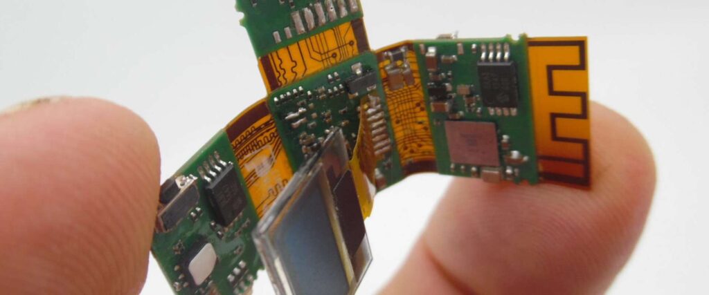
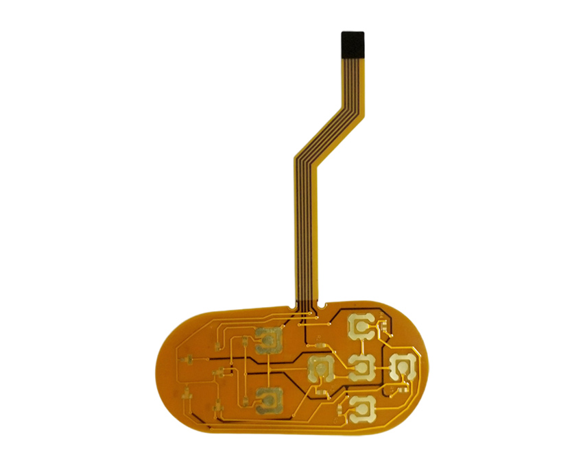
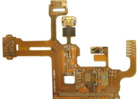
A flexible printed circuit board (flex PCB or flex circuit) is a type of printed circuit board made of flexible insulating substrate materials like polyimide or polyester. The conductive pathways are printed or laminated onto the flexible substrate.
Flex PCBs can be bent, twisted, and folded to fit into tight spaces and move dynamically in electronic devices. They are ideal for applications where flexibility, space savings, and weight reduction are critical requirements.
Key Features of Flex PCBs
- Lightweight and thin
- Can be bent, folded, twisted dynamically
- Saves space and weight in devices
- Excellent mechanical dynamism and fatigue resistance
- Can be embedded into cables and mechanisms
- Enables custom configurations and complex geometries
- Versatile integration and packaging
- Reliable connections in dynamic flexing conditions
Why Use Flexible PCBs?

There are several key advantages that make flex PCBs useful in many electronic devices:
Space Savings
Flex circuits can be bent and folded into tight spaces. This allows fitting more circuitry into a compact footprint, enabling smaller and lighter device designs. The thin profile is ideal for space-constrained electronics.
Flexibility and Dynamism
The flexible nature allows dynamic movement, vibration dampening, and installation into mechanically dynamic assemblies. Flex PCBs maintain reliable connections despite continuous motion and bending cycles.
Reduced Weight
Thin and lightweight flex PCBs help minimize the overall weight of devices like cell phones, wearables, and other portables. This improves portability and wearability.
Reliability
Flex PCBs offer excellent bend cycle life and fatigue resistance. The polymers and conductors are engineered for durability in dynamic bending applications.
Design Freedom
Circuits can be sculpted and formed into unique 3D shapes. Flex PCBs enable innovative packaging designs not possible with rigid boards.
Easier Assembly
Components can be pre-assembled on flex PCB sections for simpler, low-cost device assembly vs rigid PCBs.
In summary, the flexibility, space savings, weight reduction and durability make flex PCBs ideal for many modern portable electronic products. The design freedom also enables innovations in packaging and assembly.
Typical Applications of Flexible PCBs
Flex PCBs are widely used in the following types of electronic devices:
- Consumer electronics
- Cell phones
- Laptops
- Digital cameras
- Fitness bands, watches
- VR headsets
- Automotive electronics
- Engine control units
- In-vehicle infotainment
- Lighting, reverse cameras
- Sensors
- Medical devices
- Hearing aids
- Diagnostic instruments
- Patient monitoring
- Implants
- Industrial
- Robotics, UAVs
- Motors, actuators
- Sensors, instrumentation
- Aerospace and defense
- Avionics, guidance systems
- Radar, communication
- Missiles, weapons systems
In most cases, flex PCBs are used for:
- Interconnections between PCBs
- Connections between boards and displays
- Wiring harnesses, cables
- Components in motion assemblies
- Space-constrained electronics enclosures
- Any application requiring a thin profile or dynamic flexing capability
As electronics become more compact and complex, flex PCBs provide the interconnectivity and packaging solutions demanded in modern mobile and portable devices.
Construction and Materials Used in Flex PCBs
Flex PCBs have three key elements in their construction:
Flexible Substrate
The base of the flex PCB is a thin insulating flexible substrate or dielectric layer. The most common materials used are polyimide (PI) and polyester (PET). These provide the needed combination of flexibility, chemical resistance, temperature tolerance, and electrical insulation.
Typical thicknesses range from 12.5 to 100 micrometers. Polyimide films as thin as 6 um can be used. The thinner the substrate, the more flexible the circuit can be.
Conductors
The conducting traces that form the circuits are typically made from rolled annealed copper foil, 18 to 70 micrometers thick. The foil is bonded to the substrate, and then covered with a photoresist coating for patterning the circuits.
Other conductive materials like silver, nickel, and aluminum can also be used, but copper is most common due to its excellent conductivity and flexibility.
Cover layer
A cover layer or solder mask is applied over the traces to provide insulation, protect the copper from corrosion, and prevent shorting between lines. Flexible solder mask materials like LPI and aqueous acrylic are used.
Additionally, the circuits can be plated with immersion silver, immersion tin or other finishes to protect the copper and facilitate soldering.
Flex PCB Constructions

Flex PCBs are fabricated in many different configurations. Here are the main construction types:
Single Sided Flex Circuits
Consist of conductive traces on only one side of the substrate. Typically 1 to 2 layers. Low cost, ideal for simpler interconnections.
Double Sided Flex Circuits
Have conductor layers on both sides of the substrate. Provides routing space for more complex circuits.
Multilayer Flex Circuits
Contain 3 or more conductive layers separated by flexible dielectric films. Permits more compact routing for high density interconnections.
Rigid-Flex PCBs
Combine rigid FR-4 PCB sections with flexible polyimide sections to integrate dynamic flexing with rigid support. Allows embedding flex sections into enclosures while maintaining dynamic movement capabilities.
Flex-Rigid-Flex PCBs
Have flexible sections integrated on both sides of a central rigid section. Provides flexible interconnections from both sides of a rigid board.
Sculpted Flex Circuits
Are shaped into 3D forms. Flexible circuits can be formed to fit unique outlines and spaces.
Metal Core Flex Circuits
Use a metal foil core (like aluminum) instead of dielectric substrate for heat dissipation and EMI/RFI shielding capabilities.
Optical Flex Circuits
Add embedded fiber optic channels to flex boards for transmitting data optically. Used for high speed data transmission.
Stretchable Flex Circuits
Use specially engineered polymers to allow stretching and elastic behavior for wearables and stretchable electronics.
Flex PCB Design Considerations
Designing flex PCBs requires attention to the dynamic mechanical aspects and stress factors involved. Here are some of the key design considerations:
Dynamic Bending
- Determine the required bend radius based on flex circuit layers and materials
- Avoid sharp folds and tear drops
- Use generous curve radii at bends
- Design appropriate strain relief into terminals
Flexing Stress
- Minimize conductor widths in high flexing areas
- Use teardrop pads to reduce stress cracking
- Isolate high-stress points with slit or cutouts
- Reduce layers or use flexible solder mask and coverlay in high-flex zones
Layer Stackup
- Use thinner dielectrics for maximal flexibility
- Place ground planes near middle layer
- Use symmetrical layer sequences to balance stress
Board Stiffeners
- Add stiffening bars/ribs in rigid sections
- Prevent flexing in fragile soldered component areas
Component Placement
- Position high-profile components in rigid sections
- Use adhesives to prevent component movement/detachment
Manufacturing Process for Flex PCBs
Flex PCB fabrication involves specialized processes tailored to the flexible material properties. Here is an overview of the typical manufacturing workflow:
Design and Layout
Board designed with CAD tools. Requires planning for dynamic flexing constraints.
Film Materials Preparation
Substrate and dielectric films are cut, cleaned, undergo surface treatments.
Photolithography
Photoresist coatings applied to copper foils. Masked exposure and etching forms circuit patterns.
Lamination
Layers of substrate, adhesive and foil are stacked and laminated under heat and pressure. Crosslinking bonds the multilayer stackup.
Component Assembly
SMD components attached by reflow or adhesive methods. Stiffeners added for strengthening.
Testing and Inspection
100% electrical testing and automated optical inspection ensures quality.
Singulation
Boards are cut from panel using lasers, routers, or punch/shear tools.
Connector and Harness Assembly
Connectors crimped or soldered to boards. Flex assemblies are integrated into cable harnesses.
The specialized skills, engineering knowledge and equipment investment required make it advisable to work with an experienced flex PCB manufacturer.
Flex PCB vs Rigid PCBs
Here is a comparison between flex PCBs and rigid PCBs:
| Parameter | Flex PCB | Rigid PCB |
|---|---|---|
| Substrate | Polyimide, PET | FR4, Ceramics |
| Dielectric | 12.5 – 100 um | 100 – 200 um |
| Layers | 1- 12 | 4 – 20+ |
| Max Size | 356 x 610 mm | 610 x 1220 mm |
| Weight | Light | Heavy |
| Dynamic bending | Excellent | None |
| Environmental resistance | Good | Excellent |
| High speed design | Challenging | Preferred |
| Design complexity | Moderate | Very high |
| Cost | Moderate | Low |
In summary:
- Flex PCB provide superior flexibility, dynamism and light weight
- Rigid PCBs enable more layers and complex high density routing
- Rigid PCBs have lower costs in high volume manufacturing
- Flex PCBs cost more but provide critical space, weight and flexibility advantages
Frequently Asked Questions (FQA) about Flex PCBs
Q: How durable are flexible PCBs?
A: Flex PCBs are engineered to be extremely durable despite continual dynamic flexing. The substrate and copper conductors handle thousands of bending cycles. Flex life depends on the bend radius – tighter bends induce more strain. Careful design allows flex PCBs to achieve over 1 million bend cycles.
Q: Can components be soldered onto flex PCBs?
A: Yes, surface mount components are widely used on flex PCBs, attached through solder reflow. Adhesives can also be used in high vibration environments. Care must be taken with rigidity of components to prevent cracking. Low profile components are preferred.
Q: What are some examples of flex PCB applications?
A: Flex PCBs are used in cell phones, cameras, laptops, automotive electronics, aerospace avionics, medical devices, and industrial equipment. Any application where flexibility, dynamism, small size and light weight are important requirements.
Q: How small can flex PCB traces and spaces be fabricated?
A: Modern flex PCBs can reliably fabricate traces and spaces down to 3-5 mil (0.15 mm) using fine line photolithography and precision align/lamination equipment. Some manufacturers can achieve 2 mil lines for high density interconnects.
Q: How many layers can be made in multilayer flex circuits?
A: Up to 12 conductive layers is readily achievable with flex PCB technology today. Some manufacturers can produce flex PCBs with more than 20 layers for advanced applications demanding high interconnect density.
Q: Can flex PCBs be bent during soldering?
A: It is not recommended to bend the PCB while soldering as it can induce stress cracks in the traces. The boards should be kept rigid and planar during any soldering process. Dynamic bending should occur only during normal operation.
Q: What are some alternatives to flex PCBs for flexible electronics?
A: Alternatives include folded rigid PCBs, ribbon cables, conductive elastomers, metal foils, conductive fabric/yarns, and technologies like printed electronics or organic semiconductors. But flex PCBs remain the most mature and capable flexible interconnection technology for most applications.
Q: What safety issues should be considered with flex PCBs?
A: Thermal management is important as flex PCBs are less efficient at heat dissipation than metal-core PCBs. Also, care must be taken near cutting edges and points of flexure to prevent pinching or cuts. Proper insulation and covers are necessary.


Leave a Reply