Introduction
Printed Circuit Boards (PCBs) have revolutionized the electronics industry since their inception in the early 20th century. These thin, flat boards made of insulating material with conductive copper traces have become an integral part of almost every electronic device we use today. From smartphones and computers to medical equipment and aerospace technology, PCBs have enabled the development of increasingly complex and compact electronic systems. In this article, we will delve into the fascinating history of PCBs, tracing their evolution from early prototypes to the advanced multi-layered boards of the modern era.
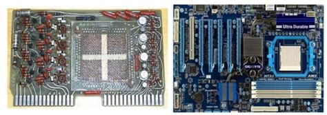
The Early Days of PCBs
The Advent of Electronic Circuits
The history of PCBs is closely tied to the development of electronic circuits. In the early days of electronics, circuits were constructed using point-to-point wiring, where components were directly connected using wires. This method was time-consuming, error-prone, and resulted in bulky and unreliable devices. As electronic systems became more complex, the need for a more efficient and compact method of circuit construction became apparent.
The First PCB Prototypes
The concept of using a printed circuit to simplify electronic assembly can be traced back to the early 1900s. In 1903, German inventor Albert Hanson filed a patent for a “printed wire” that described a method of using conductive ink to print circuits on an insulating substrate. However, this idea remained largely theoretical until the 1920s.
In 1925, Charles Ducas, an American inventor, filed a patent for a “printed wire” that described a method of printing conductive ink on an insulating substrate to create a circuit. This patent laid the groundwork for the development of modern PCBs.

The Development of PCB Technology
The Rise of Radio and the Need for Compact Circuits
The 1930s saw a significant increase in the popularity of radio technology, which created a demand for more compact and efficient electronic circuits. In response to this need, Austrian engineer Paul Eisler developed the first practical PCB in 1936. Eisler’s PCB consisted of a thin sheet of insulating material with conductive copper foil bonded to one side. The copper foil was etched away to create the desired circuit pattern, and holes were drilled to allow components to be mounted on the board.
World War II and the Advancement of PCB Manufacturing
During World War II, the demand for reliable and compact electronic systems for military applications drove the further development of PCB technology. In the United States, the National Bureau of Standards (now the National Institute of Standards and Technology) and the Radio Corporation of America (RCA) worked on refining PCB manufacturing processes.
One of the key advancements during this period was the development of the “subtractive” method of PCB manufacturing, which involved etching away unwanted copper from a fully copper-clad board to create the desired circuit pattern. This method proved to be more efficient and reliable than earlier methods, and it remains the basis for modern PCB manufacturing.
The Post-War Era and the Commercialization of PCBs
After World War II, PCB technology began to spread to commercial applications. In the 1950s, companies such as Motorola and IBM started using PCBs in their electronic products, recognizing the benefits of increased reliability and reduced manufacturing costs.
The 1960s saw the introduction of through-hole technology, which allowed components to be mounted on both sides of the PCB by inserting their leads through holes drilled in the board. This advancement further increased the density and complexity of electronic circuits that could be created using PCBs.

The Evolution of PCB Design and Manufacturing
The Introduction of Surface Mount Technology (SMT)
In the 1980s, Surface Mount Technology (SMT) began to replace through-hole technology as the dominant method of component mounting on PCBs. SMT components are smaller and can be mounted directly on the surface of the PCB, eliminating the need for drilled holes. This advancement allowed for even greater circuit density and further miniaturization of electronic devices.
The Development of Multi-Layer PCBs
As electronic systems became more complex, the need for PCBs with more than two layers arose. Multi-layer PCBs consist of multiple layers of insulating material with conductive copper traces sandwiched between them. These layers are interconnected using vias, which are small holes drilled through the board and plated with conductive material.
The development of multi-layer PCBs in the 1970s and 1980s enabled the creation of highly complex electronic systems with increased functionality and reduced size. Today, PCBs with up to 50 layers or more are not uncommon in advanced electronic applications.
Advancements in PCB Materials and Manufacturing Processes
Over the years, various advancements in PCB materials and manufacturing processes have contributed to the continued evolution of PCB technology. Some notable developments include:
-
High-frequency materials: The development of specialized PCB materials with low dielectric constants and low loss tangents has enabled the creation of High-Frequency PCBs for applications such as 5G networks and automotive radar systems.
-
Flexible PCBs: The introduction of Flexible PCB Materials has allowed for the creation of bendable and conformable electronic circuits, which are particularly useful in wearable devices and compact electronic systems.
-
Additive manufacturing: Recent advancements in additive manufacturing techniques, such as 3D printing, have opened up new possibilities for PCB fabrication, enabling the creation of complex 3D circuit structures and rapid prototyping.

The Impact of PCBs on Modern Electronics
The Proliferation of Electronic Devices
PCBs have played a crucial role in the proliferation of electronic devices in the modern world. The compact size, reliability, and cost-effectiveness of PCBs have enabled the development of increasingly sophisticated and affordable electronic products, from consumer gadgets to industrial equipment.
PCBs in the Digital Age
In the digital age, PCBs have become even more essential to the functioning of electronic systems. The high-speed digital circuits used in modern computers, smartphones, and other digital devices rely on advanced PCB designs to ensure signal integrity and minimize electromagnetic interference.
The Future of PCBs
As electronic systems continue to advance, the demand for more sophisticated and specialized PCBs is likely to grow. Some of the key trends shaping the future of PCBs include:
-
Miniaturization: The ongoing trend towards smaller, more compact electronic devices will require PCBs with ever-increasing circuit densities and smaller feature sizes.
-
Integration of embedded components: The integration of passive components, such as resistors and capacitors, directly into the PCB substrate will further increase circuit density and reduce the size of electronic assemblies.
-
Advanced materials: The development of new PCB materials with improved thermal, mechanical, and electrical properties will enable the creation of PCBs for challenging environments and high-performance applications.
-
Sustainability: As environmental concerns continue to grow, there will be an increasing focus on the development of eco-friendly PCB materials and manufacturing processes to reduce the environmental impact of electronic waste.
Frequently Asked Questions (FAQ)
-
Q: What is a Printed Circuit Board (PCB)?
A: A Printed Circuit Board (PCB) is a thin, flat board made of insulating material with conductive copper traces printed on its surface. PCBs are used to mechanically support and electrically connect electronic components using conductive pathways, tracks, or signal traces etched from copper sheets laminated onto a non-conductive substrate. -
Q: What are the main advantages of using PCBs in electronic devices?
A: The main advantages of using PCBs in electronic devices include: - Compact size and increased circuit density
- Improved reliability and reduced manufacturing errors
- Lower production costs compared to point-to-point wiring
- Easier troubleshooting and maintenance
-
Consistency and uniformity in mass production
-
Q: What is the difference between through-hole and surface mount technology (SMT)?
A: Through-hole technology involves mounting components on a PCB by inserting their leads through holes drilled in the board and soldering them on the opposite side. Surface Mount Technology (SMT), on the other hand, involves mounting components directly on the surface of the PCB without the need for drilled holes. SMT components are smaller and allow for greater circuit density compared to through-hole components. -
Q: What are multi-layer PCBs, and why are they used?
A: Multi-layer PCBs consist of multiple layers of insulating material with conductive copper traces sandwiched between them. These layers are interconnected using vias, which are small holes drilled through the board and plated with conductive material. Multi-layer PCBs are used to create highly complex electronic systems with increased functionality and reduced size, as they allow for greater circuit density and more efficient use of board space compared to single- or double-layer PCBs. -
Q: How have advancements in PCB technology influenced the development of modern electronics?
A: Advancements in PCB technology, such as the introduction of surface mount technology, the development of multi-layer PCBs, and improvements in PCB materials and manufacturing processes, have greatly influenced the development of modern electronics. These advancements have enabled the creation of increasingly compact, reliable, and sophisticated electronic devices, from smartphones and computers to medical equipment and aerospace technology. As PCB technology continues to evolve, it will play a crucial role in shaping the future of electronic systems and the devices we rely on in our daily lives.
Conclusion
The history of Printed Circuit Boards is a fascinating story of innovation, problem-solving, and technological advancement. From the early days of point-to-point wiring to the advanced multi-layer boards of the modern era, PCBs have revolutionized the way we design, manufacture, and use electronic devices. As electronic systems continue to become more complex and sophisticated, the importance of PCBs in enabling these advancements cannot be overstated.
Looking to the future, it is clear that PCBs will continue to play a crucial role in shaping the landscape of electronic technology. As new materials, manufacturing processes, and design techniques are developed, PCBs will evolve to meet the ever-increasing demands of the electronics industry. From the ongoing trend towards miniaturization to the integration of embedded components and the focus on sustainability, the future of PCBs promises to be as exciting and transformative as its past.
| Era | Key Developments |
|---|---|
| Early 1900s | Concept of printed circuits first proposed |
| 1920s-1930s | First practical PCBs developed by Paul Eisler |
| World War II | Advancement of PCB manufacturing for military applications |
| Post-War Era | Commercialization of PCBs in consumer electronics |
| 1960s | Introduction of through-hole technology |
| 1970s-1980s | Development of multi-layer PCBs |
| 1980s-Present | Widespread adoption of surface mount technology (SMT) |
Table 1: Timeline of key developments in PCB History
In conclusion, the history of Printed Circuit Boards is a testament to human ingenuity and the power of technological innovation. As we continue to push the boundaries of what is possible in electronic design and manufacturing, it is important to recognize and appreciate the crucial role that PCBs have played in bringing us to where we are today. With a deep understanding of the past and a keen eye on the future, we can continue to harness the potential of PCBs to create a more connected, efficient, and sustainable world.


Leave a Reply