Understanding Panelization dimensions
Panelization is a process in PCB manufacturing that involves grouping multiple printed circuit boards (PCBs) onto a single panel for efficient fabrication and assembly. This technique helps to reduce manufacturing costs, minimize handling, and optimize the use of materials. When designing panels for PCB production, it is crucial to consider the dimensions of the individual boards, the spacing between them, and the inclusion of breakaway tabs or Mouse Bites for easy separation.
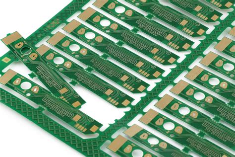
What are Breakaway Tabs and Mouse Bites?
Breakaway tabs, also known as breakoff tabs or snap-off tabs, are small protrusions added to the edges of individual PCBs within a panel. These tabs connect the boards to the main panel frame, providing stability during the manufacturing process. Once the fabrication and assembly are complete, the tabs can be easily broken off to separate the individual boards from the panel.
Mouse bites, on the other hand, are small, semi-circular cutouts placed along the perimeter of each PCB in a panel. These cutouts create a perforated line that allows for easy separation of the individual boards after manufacturing. Mouse bites are an alternative to breakaway tabs and are often preferred when a cleaner edge finish is required on the final PCBs.
Importance of Proper Panelization Dimensions
Proper panelization dimensions are essential to ensure the success of the PCB manufacturing process and the quality of the final products. Some key reasons why accurate dimensions are crucial include:
-
Manufacturing compatibility: Panels must be designed to fit within the constraints of the manufacturing equipment, such as the maximum panel size and the minimum spacing between boards.
-
Material optimization: Efficient panelization layouts help to minimize waste materials, reducing overall production costs.
-
Assembly accuracy: Proper spacing between boards and the placement of breakaway tabs or mouse bites contribute to the accuracy of the assembly process, ensuring that components are correctly placed on each PCB.
-
Ease of separation: Well-designed breakaway tabs or mouse bites allow for clean and easy separation of individual PCBs from the panel, minimizing the risk of damage during the depaneling process.
Standard Panelization Dimensions
When designing panels for PCB manufacturing, there are several standard dimensions to consider. These dimensions ensure compatibility with common fabrication and assembly equipment and help to optimize the production process.
Panel Sizes
Standard panel sizes vary depending on the manufacturing capabilities of the PCB fabricator. Some common panel sizes include:
| Panel Size | Dimensions (mm) | Dimensions (inches) |
|---|---|---|
| Small | 229 x 305 | 9 x 12 |
| Medium | 305 x 457 | 12 x 18 |
| Large | 457 x 610 | 18 x 24 |
It is essential to consult with your PCB manufacturer to determine their specific panel size capabilities and recommendations.
Board Spacing
The spacing between individual PCBs within a panel is crucial for maintaining the integrity of the boards during the manufacturing process. Adequate spacing prevents damage to the circuits and components due to vibrations or movement.
Recommended spacing between boards:
| Board Thickness | Minimum Spacing |
|---|---|
| <= 1.0 mm | 2.0 mm |
| 1.0 – 1.6 mm | 2.5 mm |
| 1.6 – 2.0 mm | 3.0 mm |
| > 2.0 mm | 3.5 mm |
Breakaway Tab Dimensions
Breakaway tabs should be designed to provide sufficient support for the individual PCBs during manufacturing while allowing for easy separation after the process is complete. The dimensions of the breakaway tabs may vary depending on the size and thickness of the PCBs.
Typical breakaway tab dimensions:
| Tab Parameter | Dimension Range |
|---|---|
| Width | 1.5 – 3.0 mm |
| Length | 3.0 – 6.0 mm |
| Height | 1.0 – 2.0 mm |
The number and placement of breakaway tabs along the edges of each PCB will depend on the board size and shape. Generally, larger boards may require more tabs to ensure stability during manufacturing.
Mouse Bite Dimensions
Mouse bites are an alternative to breakaway tabs and offer a different method for separating individual PCBs from a panel. The dimensions of mouse bites should be designed to create a clean, easy-to-break perforated line along the board edges.
Common mouse bite dimensions:
| Parameter | Dimension Range |
|---|---|
| Diameter | 0.8 – 1.2 mm |
| Pitch (spacing) | 1.0 – 2.0 mm |
| Edge clearance | 0.3 – 0.5 mm |
The diameter of the mouse bites determines the ease of separation, while the pitch and edge clearance ensure that the board edges remain intact during the manufacturing process.

Designing for Efficient Panelization
To create an efficient panelization layout, designers must consider several factors beyond the standard dimensions. These factors help to optimize material usage, minimize manufacturing costs, and ensure the quality of the final PCBs.
Board Orientation and Placement
When placing individual PCBs within a panel, consider the following:
-
Align boards in the same orientation to simplify the assembly process and minimize the risk of errors.
-
Group boards with similar designs or components to streamline the manufacturing process.
-
Position boards to maximize material utilization and minimize waste.
-
Ensure adequate spacing between boards to prevent damage during fabrication and assembly.
Panelization Techniques
There are several panelization techniques that designers can employ to optimize the layout and minimize material waste:
-
Array panelization: Arranging identical PCBs in a grid pattern to maximize the number of boards per panel.
-
Step-and-repeat panelization: Placing multiple identical PCBs in a step-and-repeat pattern, with a consistent spacing between each board.
-
Mixed panelization: Combining different PCB Designs within a single panel to optimize material usage and reduce manufacturing costs.
-
Sub-panelization: Dividing a large panel into smaller sub-panels to accommodate different PCB sizes and shapes while maintaining efficient material utilization.
Fiducial Marks and Tooling Holes
In addition to the placement of individual PCBs, designers must also consider the inclusion of fiducial marks and tooling holes in the panelization layout.
Fiducial marks are small, precisely placed features on the panel that serve as reference points for the manufacturing and assembly equipment. These marks ensure accurate alignment and positioning of the PCBs throughout the production process.
Tooling holes are larger holes placed in the corners or edges of the panel that help to secure the panel during fabrication and assembly. The size and placement of tooling holes should be based on the specifications of the manufacturing equipment.

Panelization Design Best Practices
To ensure the success of your panelization design, consider the following best practices:
-
Consult with your PCB manufacturer early in the design process to discuss their specific panelization requirements and capabilities.
-
Use a consistent board orientation and placement strategy to simplify the manufacturing process and minimize errors.
-
Optimize the panelization layout to maximize material utilization and minimize waste.
-
Include appropriate spacing between individual PCBs to prevent damage during fabrication and assembly.
-
Design breakaway tabs or mouse bites with dimensions that provide adequate support while allowing for easy separation of the boards.
-
Incorporate fiducial marks and tooling holes in the panel design to ensure accurate alignment and secure placement during manufacturing.
-
Verify the panelization design with your manufacturer before finalizing the layout to avoid potential issues or delays in production.

Frequently Asked Questions (FAQs)
- What is the difference between breakaway tabs and mouse bites?
-
Breakaway tabs are small protrusions added to the edges of individual PCBs within a panel, providing stability during manufacturing and allowing for easy separation after the process is complete. Mouse bites, on the other hand, are small, semi-circular cutouts placed along the perimeter of each PCB, creating a perforated line for easy separation.
-
How do I determine the appropriate spacing between individual PCBs in a panel?
-
The appropriate spacing between PCBs depends on factors such as the board thickness and the manufacturing equipment capabilities. Generally, thicker boards require greater spacing to prevent damage during fabrication and assembly. Consult with your PCB manufacturer for their specific recommendations.
-
Can I mix different PCB designs within a single panel?
-
Yes, mixed panelization is a technique that allows you to combine different PCB designs within a single panel to optimize material usage and reduce manufacturing costs. However, it is essential to ensure that the different designs are compatible with the manufacturing process and do not introduce complexity that could lead to errors or delays.
-
What are fiducial marks, and why are they important in panelization design?
-
Fiducial marks are small, precisely placed features on a panel that serve as reference points for the manufacturing and assembly equipment. They ensure accurate alignment and positioning of the PCBs throughout the production process, minimizing the risk of errors and improving the quality of the final products.
-
How can I optimize my panelization design to minimize material waste?
- To minimize material waste, consider using efficient panelization techniques such as array panelization, step-and-repeat panelization, or mixed panelization. These techniques help to maximize the number of PCBs per panel while minimizing the amount of unused material. Additionally, consult with your PCB manufacturer for their recommendations on optimizing the panel layout based on their specific equipment and capabilities.
Conclusion
Proper panelization dimensions are crucial for the success of PCB manufacturing and the quality of the final products. By understanding the standard dimensions for panel sizes, board spacing, breakaway tabs, and mouse bites, designers can create efficient panelization layouts that optimize material usage, minimize costs, and ensure compatibility with manufacturing processes.
When designing panels for PCB production, it is essential to consider factors such as board orientation, placement, and the inclusion of fiducial marks and tooling holes. By following best practices and collaborating closely with PCB manufacturers, designers can develop panelization layouts that streamline the fabrication and assembly process, ultimately leading to high-quality, cost-effective PCBs.


Leave a Reply