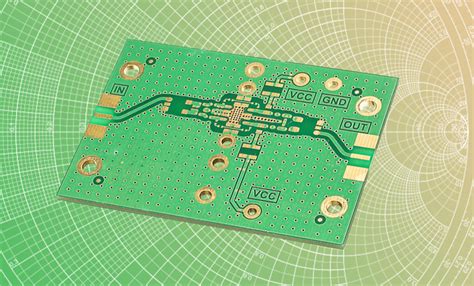
Introduction to PCB Grounding
Printed Circuit Board (PCB) grounding is a critical aspect of electronic design that ensures the proper functioning, reliability, and stability of electronic circuits. Grounding techniques involve creating a low-impedance path for electrical currents to return to their source, minimizing noise, and preventing interference between different parts of the circuit. Proper grounding is essential for maintaining signal integrity, reducing electromagnetic interference (EMI), and ensuring the overall performance of the PCB.
In this article, we will delve into the various PCB grounding techniques, their importance, and best practices for implementing effective grounding strategies in PCB Design.
The Importance of PCB Grounding
Reducing Noise and Interference
One of the primary reasons for implementing proper PCB grounding techniques is to reduce noise and interference in electronic circuits. Noise can originate from various sources, such as power supply ripple, digital switching, or external electromagnetic fields. By providing a low-impedance path for currents to return to their source, grounding helps to minimize the impact of noise on sensitive analog and digital circuits.
Ensuring Signal Integrity
Grounding plays a crucial role in maintaining signal integrity in PCBs. When signals travel through the circuit, they can be affected by factors such as impedance mismatches, reflections, and crosstalk. Proper grounding helps to establish a stable reference point for signals, reducing the impact of these factors and ensuring that signals remain clean and undistorted.
Preventing Ground Loops
Ground loops occur when there are multiple paths for ground currents to flow, leading to circulating currents and potential differences between different ground points. These ground loops can introduce noise and interference in the circuit, affecting its performance. Effective grounding techniques help to prevent ground loops by providing a single, low-impedance path for ground currents.
Enhancing Electromagnetic Compatibility (EMC)
Electromagnetic compatibility (EMC) refers to the ability of electronic devices to operate without causing or being affected by electromagnetic interference. Proper grounding is essential for achieving good EMC performance in PCBs. By minimizing the radiation of electromagnetic fields and providing shielding against external interference, grounding techniques help to ensure that the PCB meets EMC regulations and standards.

PCB Grounding Techniques
Star Grounding
Star grounding is a technique where all ground connections in a PCB are routed to a single point, known as the star point. This approach ensures that all ground currents flow through a single, low-impedance path, minimizing the potential for ground loops and voltage differences between different parts of the circuit.
To implement star grounding, designers typically create a dedicated ground plane or use a ground pour on the PCB. All ground connections are then routed to the star point using short, low-impedance traces. The star point is usually located near the power supply or the most sensitive components in the circuit.
| Advantages of Star Grounding | Disadvantages of Star Grounding |
|---|---|
| Minimizes ground loops | Requires careful planning |
| Reduces noise and interference | May increase PCB complexity |
| Improves signal integrity | Potential for ground bounce |
Multipoint Grounding
Multipoint grounding, also known as distributed grounding, involves connecting ground points at multiple locations throughout the PCB. This technique is commonly used in larger PCBs or when there are multiple ground planes.
In multipoint grounding, ground connections are made at strategic locations, such as near power supplies, sensitive components, or connectors. The goal is to provide a low-impedance path for ground currents while minimizing the distance between the ground points and the components they serve.
| Advantages of Multipoint Grounding | Disadvantages of Multipoint Grounding |
|---|---|
| Reduces ground impedance | Potential for ground loops |
| Improves signal integrity | Requires careful planning |
| Suitable for larger PCBs | May increase PCB complexity |
Ground Planes
Ground planes are large, continuous copper areas on a PCB layer that provide a low-impedance path for ground currents. They offer several benefits, including reduced impedance, improved shielding, and better heat dissipation.
When designing a PCB with a ground plane, it is important to ensure that the plane covers as much area as possible and is not unnecessarily divided or cut. Solid ground planes provide the best performance, while split planes or planes with multiple cuts can introduce impedance discontinuities and degrade signal integrity.
| Advantages of Ground Planes | Disadvantages of Ground Planes |
|---|---|
| Low impedance path | Increased PCB Fabrication cost |
| Improved shielding | May require additional layers |
| Better heat dissipation | Potential for ground bounce |
Ground Stitching and Via Stitching
Ground stitching and via stitching are techniques used to improve the electrical connection between ground planes on different layers of a PCB. Ground stitching involves placing multiple vias along the edges of ground planes to create a low-impedance connection between them. Via stitching, on the other hand, involves placing vias at regular intervals across the ground plane to ensure a consistent ground reference throughout the PCB.
These techniques help to minimize impedance discontinuities and reduce the potential for ground bounce or voltage differences between different layers. They are particularly useful in high-speed designs or when there are multiple ground planes in the PCB Stackup.
| Advantages of Ground/Via Stitching | Disadvantages of Ground/Via Stitching |
|---|---|
| Improves interlayer connection | Increases PCB manufacturing complexity |
| Reduces ground bounce | May impact signal routing |
| Minimizes voltage differences | Requires additional vias |
Grounding High-Speed Signals
High-speed signals, such as those found in digital circuits or RF applications, require special consideration when it comes to grounding. These signals are more susceptible to noise, reflections, and crosstalk, and proper grounding techniques are essential for maintaining signal integrity.
When grounding high-speed signals, it is important to use a solid ground plane and minimize the distance between the signal trace and the ground plane. This helps to reduce loop area and minimize inductance, which can cause signal degradation. Additionally, techniques such as ground stitching and via stitching can be employed to ensure a consistent ground reference throughout the PCB.
| Techniques for Grounding High-Speed Signals | Benefits |
|---|---|
| Solid ground plane | Reduces loop area and inductance |
| Minimizing signal-to-ground distance | Improves signal integrity |
| Ground stitching and via stitching | Ensures consistent ground reference |

Best Practices for PCB Grounding
Keep Ground Connections Short
To minimize impedance and reduce the potential for noise and interference, it is important to keep ground connections as short as possible. This can be achieved by placing components close to their respective ground points and using direct, low-impedance paths for ground currents.
Use Sufficient Via Size and Quantity
When connecting ground planes or routing ground connections between layers, it is important to use a sufficient number of vias with an appropriate size. Larger vias and a higher quantity of vias help to reduce impedance and improve the electrical connection between layers.
Separate Analog and Digital Grounds
In mixed-signal designs that include both analog and digital circuits, it is recommended to use separate ground planes or regions for analog and digital grounds. This helps to prevent noise from digital circuits from coupling into sensitive analog circuits. The analog and digital grounds should be connected at a single point, typically near the power supply or the analog-to-digital converter (ADC).
Use Ground Pours
Ground pours are copper areas on a PCB layer that are connected to the ground plane. They help to improve shielding, reduce impedance, and provide a low-impedance return path for currents. When creating ground pours, it is important to ensure that they are properly connected to the ground plane and do not create isolated islands or dead copper areas.
Consider Grounding in the PCB Stackup
The PCB stackup, which refers to the arrangement of layers in a PCB, plays a significant role in grounding. When designing the stackup, consider the placement of ground planes and their proximity to signal layers. In general, it is recommended to have a ground plane adjacent to each signal layer to provide a consistent reference and minimize crosstalk.

Conclusion
PCB grounding is a critical aspect of electronic design that ensures the proper functioning, reliability, and stability of electronic circuits. By implementing effective grounding techniques, such as star grounding, multipoint grounding, ground planes, ground stitching, and via stitching, designers can reduce noise and interference, ensure signal integrity, prevent ground loops, and enhance electromagnetic compatibility.
When designing PCBs, it is important to follow best practices for grounding, such as keeping ground connections short, using sufficient via size and quantity, separating analog and digital grounds, using ground pours, and considering grounding in the PCB stackup.
By understanding and applying these PCB grounding techniques and best practices, designers can create robust and reliable electronic systems that meet performance and regulatory requirements.
Frequently Asked Questions (FAQ)
1. What is the purpose of PCB grounding?
PCB grounding serves several purposes, including:
– Providing a low-impedance path for currents to return to their source
– Reducing noise and interference in electronic circuits
– Ensuring signal integrity by providing a stable reference point for signals
– Preventing ground loops and minimizing voltage differences between different parts of the circuit
– Enhancing electromagnetic compatibility (EMC) by minimizing radiation and providing shielding against external interference
2. What is the difference between star grounding and multipoint grounding?
Star grounding involves routing all ground connections to a single point, known as the star point, to create a single, low-impedance path for ground currents. This technique minimizes ground loops and voltage differences between different parts of the circuit.
Multipoint grounding, also known as distributed grounding, involves connecting ground points at multiple locations throughout the PCB. This technique is commonly used in larger PCBs or when there are multiple ground planes. It reduces ground impedance and improves signal integrity but requires careful planning to avoid ground loops.
3. Why are ground planes important in PCB design?
Ground planes are large, continuous copper areas on a PCB layer that provide a low-impedance path for ground currents. They offer several benefits, including:
– Reduced impedance, which helps to minimize noise and interference
– Improved shielding against electromagnetic interference (EMI)
– Better heat dissipation, which enhances the thermal performance of the PCB
Ground planes also provide a consistent reference for signals, helping to maintain signal integrity throughout the circuit.
4. What are ground stitching and via stitching, and why are they used?
Ground stitching and via stitching are techniques used to improve the electrical connection between ground planes on different layers of a PCB.
Ground stitching involves placing multiple vias along the edges of ground planes to create a low-impedance connection between them. This technique helps to minimize impedance discontinuities and reduce the potential for ground bounce or voltage differences between different layers.
Via stitching involves placing vias at regular intervals across the ground plane to ensure a consistent ground reference throughout the PCB. This technique is particularly useful in high-speed designs or when there are multiple ground planes in the PCB stackup.
5. What are some best practices for PCB grounding?
Some best practices for PCB grounding include:
– Keeping ground connections as short as possible to minimize impedance and reduce noise and interference
– Using a sufficient number of vias with an appropriate size to reduce impedance and improve electrical connections between layers
– Separating analog and digital grounds in mixed-signal designs to prevent noise coupling from digital to analog circuits
– Using ground pours to improve shielding, reduce impedance, and provide a low-impedance return path for currents
– Considering grounding in the PCB stackup, ensuring that ground planes are adjacent to signal layers to provide a consistent reference and minimize crosstalk
By following these best practices, designers can create robust and reliable PCBs with effective grounding that ensures proper functioning and performance of electronic circuits.


Leave a Reply