Introduction to TL07x Operational Amplifiers
The TL071, TL072, and TL074 are popular low-noise JFET-input operational amplifiers (op-amps) widely used in various analog circuit applications. These op-amps offer excellent performance characteristics, such as low input bias current, low noise, and high slew rate, making them suitable for a wide range of designs, including audio, instrumentation, and control systems.
Key Features of TL07x Op-Amps
- Low noise: TL07x op-amps have low input noise voltage, typically around 18 nV/√Hz at 1 kHz, ensuring minimal noise interference in sensitive applications.
- High Input Impedance: The JFET-input stage provides high input impedance, typically around 10^12 Ω, minimizing loading effects on the input signal.
- Low input bias current: With input bias currents in the pA range, TL07x op-amps are suitable for applications involving high-impedance sources.
- Wide bandwidth: TL07x op-amps have a unity-gain bandwidth of around 3 MHz, allowing for efficient operation in various frequency ranges.
- High slew rate: The slew rate of TL07x op-amps is typically around 13 V/μs, enabling fast signal processing without significant distortion.
Differences between TL071, TL072, and TL074
The main difference between these op-amps is the number of amplifiers per package:
- TL071: Single op-amp package
- TL072: Dual op-amp package
- TL074: Quad op-amp package
Having multiple op-amps in a single package can be advantageous in terms of board space and cost reduction, especially when designing circuits that require several op-amps.
Basic TL07x Circuit Configurations
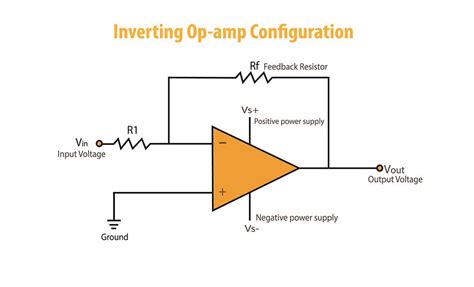
Inverting Amplifier
An inverting amplifier using a TL07x op-amp can be designed using the following Circuit diagram:
       +Vcc
        |
        |
     _____
    |     |
    |  ___|___
    | |       |
Vin-|-|R1     |
    | |       |
    |  ───┬───
    |_____|
        |
        |
       -|+
      __|__
     |     |
     |TL07x|
     |_____|
   -|+    _|_
     |     | RL
     |_____|
        |
        |
       GND
The gain of the inverting amplifier is given by:
Gain = -Rf / R1
where Rf is the feedback resistor and R1 is the input resistor.
Non-Inverting Amplifier
A non-inverting amplifier using a TL07x op-amp can be designed using the following circuit diagram:
       +Vcc
        |
        |
     _____
    |     |
    |  ___|___
    | |       |
    |-|R1     |
    | |       |
    |  ───┬───
    |_____|
        |
        |
   +|─  ─|─
    |    |
Vin-    _|_
    |    | RL
    |____|
        |
        |
       GND
The gain of the non-inverting amplifier is given by:
Gain = 1 + Rf / R1
where Rf is the feedback resistor and R1 is the input resistor.
Voltage Follower (Buffer)
A voltage follower, also known as a buffer, using a TL07x op-amp can be designed using the following circuit diagram:
       +Vcc
        |
        |
     _____
    |     |
    |     |
    |     |
    |     |
    |     |
    |_____|
        |
        |
   +|─  ─|─
    |    |
Vin-    _|_
    |    | RL
    |____|
        |
        |
       GND
A voltage follower has a gain of 1, providing high input impedance and low output impedance, making it useful for isolating stages or driving low-impedance loads without affecting the input signal.

Advanced TL07x Circuit Applications
Active Filters
TL07x op-amps can be used to design various types of active filters, such as low-pass, high-pass, band-pass, and band-stop filters. These filters can be implemented using different topologies, including Sallen-Key, Multiple Feedback (MFB), and State Variable Filters (SVF).
For example, a second-order Sallen-Key low-pass filter using a TL07x op-amp can be designed using the following circuit diagram:
       +Vcc
        |
        |
     _____
    |     |
    |  ___|
    | |  R1
Vin-|-|   |
    | |   |
    |  ───┴── C1
    |_____|   |
        |     |
        |    _|_
       -|+  _\_/_
      __|__|     |
     |     |     |
     |TL07x|     |
     |_____|     |
   -|+    _|_    |
     |     | R2  |
     |_____|     |
        |       _|_
        |        | C2
        |_________|
        |
       GND
The cutoff frequency (fc) and Q factor of the Sallen-Key low-pass filter can be calculated using the following equations:
fc = 1 / (2π√(R1 × R2 × C1 × C2))
Q = √((R1 × R2 × C1 × C2) / ((R1 + R2) × C2))
Precision Rectifiers
TL07x op-amps can be used to design precision rectifiers, which are circuits that accurately convert AC signals to DC signals. A simple half-wave precision rectifier using a TL07x op-amp can be designed using the following circuit diagram:
       +Vcc
        |
        |
     _____
    |     |
    |  ___|___
    | |       |
Vin-|-|R1     |
    | |       |
    |  ───┬───
    |_____|
        |
        |  D1
       -|+─|>|─
      __|__
     |     |
     |TL07x|
     |_____|
   -|+    _|_
     |     | RL
     |_____|
        |
        |
       GND
In this circuit, the op-amp is configured as a non-inverting amplifier with the diode D1 in the feedback loop. When the input signal is positive, the op-amp amplifies the signal, and the diode conducts, allowing the output to follow the input. When the input signal is negative, the diode is reverse-biased, and the output remains at 0 V.
Instrumentation Amplifiers
Instrumentation amplifiers are used to amplify small differential signals while rejecting common-mode noise. TL07x op-amps can be used to design instrumentation amplifiers by combining three op-amps in a specific configuration.
A basic instrumentation amplifier using TL07x op-amps can be designed using the following circuit diagram:
       +Vcc
        |
        |
     _____
    |     |
    |  ___|___
    | |       |
    |-|R1     |
    | |       |
    |  ───┬───
    |_____|
        |
        |
   +|─  ─|─
    |    |
V1 -   _|_
    |    | R3
    |____|
        |
        |
       GND

       +Vcc
        |
        |
     _____
    |     |
    |  ___|___
    | |       |
    |-|R2     |
    | |       |
    |  ───┬───
    |_____|
        |
        |
   -|+  +|─
    |    |
V2 -   _|_
    |    | R4
    |____|
        |
        |
       GND

       +Vcc
        |
        |
     _____
    |     |
    |  ___|___
    | |       |
    |-|R5     |
    | |       |
    |  ───┬───
    |_____|
        |
        |
   -|+  ─|─
    |    |
   -   _|_
    |    | RL
    |____|
        |
        |
       GND
The gain of the instrumentation amplifier is given by:
Gain = (1 + 2R1 / R3) × (R5 / R2)
where R1, R2, R3, R4, and R5 are the Resistor Values in the circuit.

TL07x Circuit Design Considerations
Power Supply Decoupling
Proper power supply decoupling is essential to ensure stable operation and minimize noise in TL07x circuits. Decoupling capacitors should be placed close to the power supply pins of the op-amp. A typical decoupling scheme involves using a 0.1 μF ceramic capacitor in parallel with a 1-10 μF electrolytic capacitor.
Input and Output Filtering
In applications where noise is a concern, input and output filtering can be employed to minimize the effects of unwanted signals. Low-pass filters can be used to attenuate high-frequency noise, while high-pass filters can be used to remove DC offsets or low-frequency noise.
PCB Layout Considerations
Proper PCB layout is crucial for optimal performance of TL07x circuits. Some key considerations include:
- Keeping signal traces as short as possible to minimize parasitic capacitance and inductance.
- Separating analog and digital grounds to prevent digital noise from coupling into analog signals.
- Using ground planes to provide a low-impedance return path for signals.
- Placing decoupling capacitors close to the op-amp power supply pins to minimize supply noise.

Frequently Asked Questions (FAQ)
1. What is the difference between TL071, TL072, and TL074 op-amps?
The main difference between these op-amps is the number of amplifiers per package. TL071 has a single op-amp, TL072 has two op-amps, and TL074 has four op-amps in a single package.
2. Can TL07x op-amps be used in single-supply applications?
Yes, TL07x op-amps can be used in single-supply applications, provided that the input and output signals are within the supply voltage range. In single-supply applications, the op-amp’s reference voltage should be set to half the supply voltage to allow for maximum signal swing.
3. What is the maximum supply voltage for TL07x op-amps?
The maximum supply voltage for TL07x op-amps is typically ±18 V. However, it is essential to consult the manufacturer’s datasheet for the specific device to ensure proper operation and to avoid damage to the op-amp.
4. How can I reduce the offset voltage in TL07x circuits?
Offset voltage can be reduced by using a potentiometer to adjust the balance between the op-amp’s input pins. This technique, known as offset nulling, involves connecting a potentiometer between the offset null pins of the op-amp and adjusting it to minimize the output offset voltage.
5. What is the purpose of the compensating pin (pin 5) in TL07x op-amps?
The compensating pin (pin 5) in TL07x op-amps is used for external frequency compensation. By connecting a capacitor between the compensating pin and the output pin, the op-amp’s frequency response can be tailored to ensure stability and optimize performance for specific applications.
Conclusion
The TL071, TL072, and TL074 op-amps are versatile and widely used in various analog circuit applications due to their excellent performance characteristics, such as low noise, high input impedance, and wide bandwidth. By understanding the basic configurations and design considerations for these op-amps, engineers and hobbyists can create efficient and reliable circuits for a wide range of applications, including audio, instrumentation, and control systems.


Leave a Reply