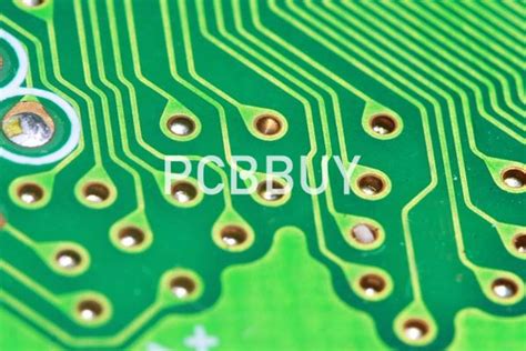
What Are PCB Vias?
PCB vias are small holes drilled through a printed circuit board that allow electrical connections between different layers of the board. Vias are essential components in PCB Design as they enable compact and complex circuit routing in a limited space. By using vias, designers can create multi-layer PCBs with intricate interconnections while minimizing the board’s overall size.
Types of PCB Vias
There are several types of PCB vias, each with its own characteristics and applications. The main types of vias are:
- Through-hole vias
- Blind vias
- Buried vias
- Micro vias
- Via-in-pad
Through-hole Vias
Through-hole vias are the most common type of via used in PCB design. They are drilled completely through the PCB, from the top layer to the bottom layer, allowing electrical connections between all layers of the board. Through-hole vias are typically plated with a conductive material, such as copper, to ensure reliable electrical connections.
Advantages of through-hole vias:
– Easy to manufacture
– Provide strong mechanical support
– Suitable for high-current applications
Disadvantages of through-hole vias:
– Consume more board space compared to other via types
– Limit the routing options on inner layers
– May cause signal integrity issues at high frequencies
Blind Vias
Blind vias are drilled from one side of the PCB and terminate at a specific inner layer without reaching the opposite side of the board. These vias are used to connect an outer layer to one or more inner layers, allowing for more compact and flexible routing.
Advantages of blind vias:
– Save board space by eliminating the need for through-hole vias
– Improve signal integrity by reducing via stubs
– Enable higher component density on the outer layers
Disadvantages of blind vias:
– More expensive to manufacture compared to through-hole vias
– Require precise drilling and plating processes
– Limited to connecting outer layers to inner layers
Buried Vias
Buried vias are located entirely within the inner layers of a PCB and do not extend to either the top or bottom layer. These vias are used to connect two or more inner layers without interfering with the outer layer routing.
Advantages of buried vias:
– Maximize board space utilization
– Reduce signal interference between layers
– Enable complex routing in high-density designs
Disadvantages of buried vias:
– Higher manufacturing costs due to specialized processes
– Difficult to inspect and repair
– Limited to connecting inner layers only
Micro Vias
Micro vias are small-diameter vias, typically less than 150 microns (0.15mm), used for high-density interconnects in advanced PCB designs. These vias are often laser-drilled and can be stacked to create complex 3D structures.
Advantages of micro vias:
– Enable high-density interconnects in compact designs
– Minimize signal distortion and crosstalk
– Suitable for high-speed and high-frequency applications
Disadvantages of micro vias:
– Require specialized manufacturing processes and equipment
– Higher cost compared to larger via types
– Potential reliability issues if not designed and manufactured properly
Via-in-Pad
Via-in-pad is a technique where a via is placed directly on a component pad, allowing for direct connection between the component and the inner layers of the PCB. This method is often used in high-density designs to save board space and improve signal integrity.
Advantages of via-in-pad:
– Reduces board size by eliminating the need for separate vias and traces
– Improves signal integrity by minimizing the distance between the component and the via
– Enables higher component density and more compact designs
Disadvantages of via-in-pad:
– Requires precise manufacturing processes to ensure proper via placement and filling
– May cause soldering issues if not properly designed and manufactured
– Limited to certain component types and sizes

Comparing PCB Via Types
| Via Type | Connects | Manufacturing Cost | Signal Integrity | Board Space |
|---|---|---|---|---|
| Through-hole | All layers | Low | Moderate | High |
| Blind | Outer to inner layers | Moderate | High | Moderate |
| Buried | Inner layers only | High | High | Low |
| Micro | High-density interconnects | High | Very high | Very low |
| Via-in-pad | Component to inner layers | Moderate | High | Very low |

Choosing the Right PCB Via Type
When selecting the appropriate via type for your PCB design, consider the following factors:
- Board complexity and layer count
- Signal integrity requirements
- Component density and board space constraints
- Manufacturing capabilities and cost
For simple, low-layer count designs, through-hole vias may suffice. However, as board complexity increases and signal integrity becomes critical, blind, buried, and micro vias may be necessary to achieve the desired performance and functionality.

Best Practices for PCB Via Design
To ensure optimal performance and reliability of your PCB, follow these best practices when designing vias:
- Minimize via count to reduce manufacturing costs and improve signal integrity
- Use appropriate via sizes and pad diameters based on the current and signal requirements
- Avoid placing vias in high-stress areas, such as near the edges of the board or under large components
- Follow the manufacturer’s guidelines for via drilling, plating, and filling processes
- Conduct thorough testing and inspection to verify via integrity and connectivity
Frequently Asked Questions (FAQ)
1. What is the difference between a through-hole via and a blind via?
A through-hole via passes through all layers of the PCB, while a blind via connects an outer layer to one or more inner layers without reaching the opposite side of the board.
2. Can micro vias be used in all PCB designs?
Micro vias are primarily used in high-density, high-speed, and high-frequency applications. They may not be necessary or cost-effective for simpler, low-layer count designs.
3. What are the advantages of using via-in-pad?
Via-in-pad reduces board size, improves signal integrity, and enables higher component density by placing vias directly on component pads.
4. How do buried vias affect PCB Manufacturing Costs?
Buried vias require specialized manufacturing processes and increase the overall cost of the PCB compared to through-hole vias.
5. What factors should I consider when choosing a via type for my PCB design?
When selecting a via type, consider the board complexity, signal integrity requirements, component density, board space constraints, and manufacturing capabilities and costs.
Conclusion
PCB vias are essential components in modern PCB design, enabling compact and complex circuit routing in multi-layer boards. Understanding the different types of vias, their advantages and disadvantages, and the best practices for via design is crucial for creating high-performance, reliable PCBs. By selecting the appropriate via type and following proper design guidelines, you can optimize your PCB’s functionality, signal integrity, and manufacturability while minimizing costs and board space.


Leave a Reply